
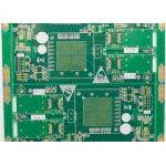
ROHS 4OZ HDI PCB Board Motherboard Printed Circuit Board
|


Fr4 Circuit Board Motherboard HF Multilayer ROHS HDI PCB Board
HDI PCB Board Introduction
HDI PCB Board is the High-Density Interconnect (HDI) Printed Circuit Boards. There is little space between the PCB components, making the board space smaller, at the same time the board functionally isn’t affected. That is, a PCB with about 120 – 160 pins per square inch is an HDI PCB. HDI boards technologies, grow fastest in PCBs, are now available for my partners. HDI Board contains blind and buried vias and often contain microvias of 0.006 or less in diameter. HDI board has higher circuitry density than traditional circuit boards.
PCB CAPABILITIES
The types of HDI PCB
Work flow for HDI
Board Cut - Inner Wet film -DES - AOI - Brown Oxido - Outer Layer Press - Out Layer Lamination - X-RAY & Rounting - Copper reduce & brown oxide - Laser Drilling - Drilling - Desmear PTH - Panel plating - Outer Layer dry film - Etching - AOI- Impedance Testing - S/M Pluged hole - Solder Mask - Component Mark - Impedance testing - Immersion Gold -V-cut - Routing - Electrical Test - FQC - FQA -Package -Shipment
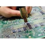
PCB Assembly Process
Similar products
Delivery Time
HDI PCB Board Application Field
Our products are widely used in communication equipment, industrial control, consumer electronics, medical equipment, aerospace, light-emitting diode lighting, automotive electronics etc.
Workshop
Common packaging
1.PCB: Vacuum packaging with carton box
Our advantage
1.Service value Independent quotation system to quickly serve the market 2.PCB manufacturing High-tech PCB and PCB assembly production line 3.Material purchasing A team of experienced electronic component procurement engineers 4.SMT post soldering Dust-free workshop, high-end SMT patch processing
Company information
We have profuse experience in manufacturing PCB,owned experienced technical R & D technology team, young and professional sales and customer service team, experienced and professional procurement team and assembly testing team, which make sure the products quality of the pass rate, on-time delivery rate of customer orders. Our services include: circuit board design and layout, 2-46 layers PCB manufacturing, professional FPC production, electronic components purchasing, SMT professional processing, Soldering and Assembly, especially sample and small bulk orders. we have the advantages of a quick quote, fast production, fast delivery.
|
||||||||||||||||||||||||||||||||||||||||||||||||||||||||||||||||||||||||||||||||||||||||||||||||||||||||||||||||||||||||||
| Product Tags: 4OZ HDI PCB Board ROHS HDI PCB Board HDI Motherboard Printed Circuit Board | ||||||||||||||||||||||||||||||||||||||||||||||||||||||||||||||||||||||||||||||||||||||||||||||||||||||||||||||||||||||||||
|
Blind Buried Vias Hole High Density PCB HDI PCB Stackup |

|
Fr-4 6 Layer Hdi Pcb Manufacturing Service For Communications |

|
1.6mm Multi-Layers Hdi Pcb Board 53.7*56mm Size |
|
Green High End Hdi Pcb Board For Automotive Electronics |

|
94v0 1oz Enig Hdi Pcb Board 4layer Oem Fabricating |

|
Buried Vias Enig Oem Pcb Board Multi-Layering 1oz Hdi |