
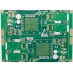
Double Sided SMT DIP 2oz HDI Printed Circuit Boards
|


Fr4 PCB Board Double Sided Printed Circuit Board SMT DIP HDI Printed Circuit BoardsHDI PCB Board Introduction
HDI PCB Board Manufacturing also known as high-density interconnect PCB, is a kind of PCB with a higher wiring density per unit area than traditional boards. HDI boards are more compact and have smaller vias, pads, copper traces and spaces. As a result, HDIs have denser wiring resulting in lighter weight, more compact, lower layer count PCBs. HDI PCB is more fit into the little spaces and have a smaller amount of mass than conservative PCB designs.
Factory Capabilities
The types of HDI PCB
Work flow for HDI
Board Cut - Inner Wet film -DES - AOI - Brown Oxido - Outer Layer Press - Out Layer Lamination - X-RAY & Rounting - Copper reduce & brown oxide - Laser Drilling - Drilling - Desmear PTH - Panel plating - Outer Layer dry film - Etching - AOI- Impedance Testing - S/M Pluged hole - Solder Mask - Component Mark - Impedance testing - Immersion Gold -V-cut - Routing - Electrical Test - FQC - FQA -Package -Shipment
Our Service
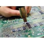
WorkShop
Advantages of HDI PCB
1.High Component Density
HDI PCB Application FieldHDI PCB board are mainly used for many industries , Like : Automotive ; aerospace industries;medical devices;Industrial automation,etc .
Except mentioned above, you'll also can find high-density interconnect PCBs in all types of digital devices, like smartphones and tablets, in automobiles, aircraft , mobile /cellular phones, touch-screen devices, laptop computers, digital cameras, 4/5G network communications, and military applications such as avionics and smart munitions.
Partners
Common packaging
Company InformationBeijing Haina lean Electronics Co.,Ltd is one of the most professional PCB manufacture in Beijing,China. With more then 10 years of development, Haina Lean Electronics turns into a first class manufacture of HDI PCB ,with production capability 4000 square meters. Our factory is providing high quality bare PCB, PCB layout design service and PCB assembly service,including components sourcing, function test,conformal coating and complete assembly for clients all.
|
|||||||||||||||||||||||||||||||||||||||||||||||||
| Product Tags: 2oz HDI printed circuit boards SMT DIP HDI printed circuit boards HDI high density circuit board |
|
Blind Buried Vias Hole High Density PCB HDI PCB Stackup |

|
Fr-4 6 Layer Hdi Pcb Manufacturing Service For Communications |

|
1.6mm Multi-Layers Hdi Pcb Board 53.7*56mm Size |
|
Green High End Hdi Pcb Board For Automotive Electronics |

|
94v0 1oz Enig Hdi Pcb Board 4layer Oem Fabricating |

|
Buried Vias Enig Oem Pcb Board Multi-Layering 1oz Hdi |