
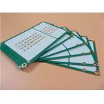
TF600 PCB 2-layer 25mil High-Frequency Substrate with Copper-filled
|


|
This 2-layer rigid PCB is fabricated from TF600, a thermosetting high-frequency laminate composed of modified PTFE resin and micron-sized ceramic fillers. It features 0.7mm finished thickness, 1 oz (1.4 mils) outer copper cladding, ENIG surface finish, and copper-filled vias on specified IC pads, ensuring superior signal integrity, thermal stability, and long-term reliability for high-frequency systems.
PCB Specifications
PCB Stack-Up Configuration This 2-layer rigid PCB features a symmetric stack-up structure, with detailed layer specifications outlined below (ordered from top to bottom):
Artwork Format and Quality Compliance The Gerber RS-274-X format is formally designated as the artwork standard for this PCB, ensuring seamless compatibility with professional PCB design software and automated manufacturing equipment throughout the production process. This PCB strictly complies with the IPC-Class-2 quality standard, which establishes rigorous specifications for performance, reliability, and manufacturing consistency, thereby validating its applicability in high-reliability RF and microwave applications.
Global Availability This high-performance PCB is available for global shipment. It is suitable for both prototyping and large-volume production orders, ensuring convenient accessibility and timely delivery to customers worldwide.
TF600 Substrate Introduction TF600 is a thermosetting high-frequency laminate consisting of modified PTFE resin and micron-sized ceramic fillers, offering excellent microwave performance and temperature resistance. It strikes a balance between ultra-low dielectric loss, stable DK consistency, and FR4-compatible processing—including drilling, plating, and lamination—and supports 260℃ lead-free assembly. Boasting superior thermal stability and moisture resistance, TF600 contains no glass fiber cloth and is well-suited for high-reliability RF and microwave designs where low insertion loss and signal integrity are critical.
TF600 Key Features and Benefits
Typical Applications
PTFE Ceramic Composite Dielectric Substrate TF-1/2 and TF600 This product is composed of PTFE resin material, which offers excellent microwave properties and temperature resistance, combined with ceramics. The material contains no glass fiber fabric. The dielectric constant is precisely adjusted by varying the ratio between ceramic and PTFE resin. The production process is unique, resulting in superior dielectric performance and high reliability. "TF" refers to the non-clad (uncoppered) smooth surface material, "TF-1" refers to single-sided copper-clad material, and "TF-2" refers to double-sided copper-clad material.
Product Features
|
||||||||||||||||||||||||||||||||||||||||||||||||||||||||||||||||
| Product Tags: AD255C PCB high frequency laminate copper clad sheet PCB material high frequency copper clad laminates |

|
2-Layer WL-CT350 4mil Ultra--thin PCB Laminate with Immersion Gold Finish |

|
Double-sided 7.5mil TLY-5 Material Ultra-Low Loss Millimeter Wave PCB |
|
2-Layer TFA300 PCB on 5mil High-Frequency Substrate |

|
Copper Coin Embedded PCB 6-Layer M6+High TG FR4 |

|
Double-Sided CER-10 High-Frequency PCB 30mil Laminate Immersion Silver |

|
2-layer TFA294 PCB Low-loss Microwave Circuits with Immersion Gold |