China Sapphire Optical Window manufacturer
Chongqing Silian Optoelectronic Science & Technology Co., Ltd.
5
Home > Products > Sapphire Semiconductor >

Gallium Nitride On Sapphire Semiconductor GaN 100mm

Browse Categories

Chongqing Silian Optoelectronic Science & Technology Co., Ltd.

City: chongqing

Province/State:chongqing

Country/Region:china

Tel:86--4008310499

Contact Person:
Ms.Wu
View Contact Details

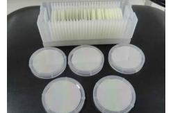
Gallium Nitride On Sapphire Semiconductor GaN 100mm

Brand Name Silian
Model Number Customized
Certification SGS/ ISO/RoHs
Place of Origin China
Minimum Order Quantity 5 pcs
Price by case
Payment Terms T/T, Western Union, MoneyGram
Supply Ability 20,000 pcs/month
Delivery Time 5-8 weeks
Packaging Details 1pcs/12pcs/25 pcs
product name gan on sapphire wafers
diameter 100mm
color transparent
matarial AL2O3
partical 10
thickness 430um
Detailed Product Description

Gallium Nitride on Sapphire Wafers (GaN)


We grow are sapphire wafers using several methods

  • Czrochroski (CZ) process is known to be more efficient for c-axis sapphire substrate production.
  • Heat Exchanger Method (HEM) - Used to grow sapphire crystal in volume.
  • Kyropoulos (KY) - grows high quality sapphire but requires an enormous amount of electricity.
  • Edge defined, Film-fed (EFG) - FG technique. A crystal growth process to manufacture more than 10 crystals at one time up to 1.5mm thick per crystal using multi-tip EFG


Sapphire grown using the CZ, HEM or KY methods is used for increasing and expand the production, capacity. EFG are usually used for small volume production.


Sapphire Semiconductor Substrates are available in all Orientations


Orientations include: R-axis; A-axis; C-axis;M-axis.

Sapphire substrates are available in various shapes (circular, rectangle, or square), from a few mm up to 200mm in size, and finishes according to customer specification. Primary flats(as per industry standards) are provided on circular substrates for orientation purposes; secondary flats are available on request. Substrate thickness' range from 0.013" (0.25mm) to 0.025" (0.675mm), depending on your particular application requirements.
We have wafers in stock!

Specs we can provide:

50.8mm 430um SSP and DSP C-M 0.2 Deg

50.8mm 100um SSP and DSP C-plane off to M Plane 0.2 Deg

50.8mm - Other specs and orienations available

100mm 650um SSP

100mm MECH GRADE - LOW PRICE!

Other diameters from but not limited to 10mm x 10mm, 76.2mm, 150mm and 200mm.

Sapphire Wafers for MOCVD growth of Gallium Nitride (GaN) Thin-Films

Clients requests sapphire substrates for to grow MOCVD Growth.

Pls see below for the offer,and see the attached for the manufacturer details and brochures

1. Crystal Materials: 99.995 (or equivalent), High Purity, Monocrystalline Al2O3.
2. Orientation: M-plane (1-100) Patterned Sapphire Substrate (PSS)
3: Diameter: 50.8 mm ± 0.1 mm (2 inch standard diameter).
4. Thickness: 430 μm ± 25 μm (or equivalent).
5. Primary Orientation Flat (OF): A-plane (1 1 -2 0) ± 0.2° (or equivalent).
6. Secondary Orientation Flat: NO
7. Front Surface: Epi-polished, Ra 0.3 nm (by AFM) (or better).
8. Back Surface: Fine-ground, Ra =0.5 - 1.2 um (or equivalent).
9. PSS Shape: Cone
10. PSS Dimension: Height 1.5 um, Diameter 1.2-1.8 um, Pitch 1.2-1.8 um.
11. Packaging: Class 100 clean room and vacuum packaging.
12. Packaging Quantity: 25 pieces per cassette.
13. Product Origin: Taiwan . see attached for the manufacturer details and brochures.
14. M-PSS wafers are to be used for MOCVD growth of gallium nitride (GaN) thin-films.
15. Qty. [50 Unit ]

Pelase contact us for pricing.


Product Tags: Sapphire Semiconductor 100mm   Sapphire Semiconductor GaN   gan on sapphire wafers  
Related Products
Email to this supplier
 
From:
Enter your Email please.
To: Chongqing Silian Optoelectronic Science & Technology Co., Ltd.
Subject:
Message:
Characters Remaining: (80/3000)