
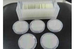
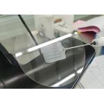
Gallium Nitride On Sapphire Semiconductor GaN 100mm
|
|
Gallium Nitride on Sapphire Wafers (GaN)
We grow are sapphire wafers using several methods
Sapphire grown using the CZ, HEM or KY methods is used for increasing and expand the production, capacity. EFG are usually used for small volume production.
Sapphire Semiconductor Substrates are available in all Orientations
Orientations include: R-axis; A-axis; C-axis;M-axis. Sapphire substrates are available in various shapes (circular, rectangle, or square),
from a few mm up to 200mm in size, and finishes according to
customer specification. Primary flats(as per industry standards)
are provided on circular substrates for orientation purposes;
secondary flats are available on request. Substrate thickness'
range from 0.013" (0.25mm) to 0.025" (0.675mm), depending on your
particular application requirements. Specs we can provide: 50.8mm 430um SSP and DSP C-M 0.2 Deg 50.8mm 100um SSP and DSP C-plane off to M Plane 0.2 Deg 50.8mm - Other specs and orienations available 100mm 650um SSP 100mm MECH GRADE - LOW PRICE! Other diameters from but not limited to 10mm x 10mm, 76.2mm, 150mm and 200mm. Sapphire Wafers for MOCVD growth of Gallium Nitride (GaN) Thin-Films Clients requests sapphire substrates for to grow MOCVD Growth. Pls see below for the offer,and see the attached for the manufacturer details and brochures 1. Crystal Materials: 99.995 (or equivalent), High Purity,
Monocrystalline Al2O3. Pelase contact us for pricing.
|
| Product Tags: Sapphire Semiconductor 100mm Sapphire Semiconductor GaN gan on sapphire wafers |
|
Gallium Nitride On Sapphire Semiconductor GaN 100mm |
|
M Plane Sapphire Semiconductor 430um High Crystal Purity |
|
A Plane Sapphire Semiconductor , Transparent 2 Inch DSP Wafer |
|
OEM C Plane Sapphire Semiconductor 0.05 Directional Accuracy |
|
|
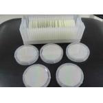
Gallium Nitride On Sapphire Semiconductor GaN 100mm |
|
|
M Plane Sapphire Semiconductor 430um High Crystal Purity |