
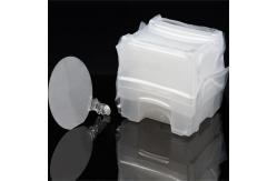
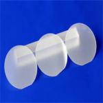
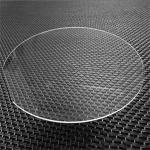
100mm 4 Inch Single Crystal Sapphire Wafer High Mechanical Strength
|


|
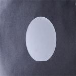
4 Inch Sapphire Substrate Is Widely Used
Product DescriptionThe epitaxial layers of GaN-based materials and devices are mainly grown on sapphire substrates. Sapphire substrate has many advantages: firstly, the production technology of sapphire substrate is mature and the device quality is good; secondly, sapphire is very stable and can be used in the high-temperature growth process; finally, sapphire has high mechanical strength and is easy to handle And cleaning. Therefore, most processes generally use sapphire as the substrate.
Technical Specification
Working principle
The working principle of the LED is that in the case of forward conduction, the electrons and holes injected into the P/N section of the diode meet and recombine, and the potential energy is converted into light energy. The wavelength of the emitted photons (that is, the color of light) is determined by the energy band width of the semiconductor. The current blue and green LED devices are based on group III nitride semiconductors, which is mainly GaN, and InNAlN is the supplementary four. Yuan AlGaInN alloy system. To epitaxially grow a GaN film on a sapphire substrate, firstly a two-step epitaxial GaN buffer layer on the substrate (low-temperature epitaxial GaN nucleation layer, then high-temperature epitaxial u-GaN buffer layer); the second step is to grow Si-doped n-GaN The third step is to grow a multifunctional quantum well to provide a radiation recombination center, allowing electrons and holes to recombine and emit light; the fourth step to grow a Mg-doped p-GaN layer to provide hole injection. Normally, the LED structure is as shown in the picture.
|
|||||||||||||||||||||||||||||||||||||||||||||||||||||||||||||||||||||||||||||||||||||||||||||
| Product Tags: SGS 4 Inch single crystal sapphire wafer SGS 100mm single crystal sapphire wafer SGS 4 inch sapphire wafer | |||||||||||||||||||||||||||||||||||||||||||||||||||||||||||||||||||||||||||||||||||||||||||||
|
4 Inch LED Sapphire Substrate , Custom Sapphire Glass Wide Transmission Range |
|
High Purity Single Crystal Sapphire Substrates 200mm |
|
2 Inch LED Sapphire Substrate For High End Lighting |
|
No Cracking 6 Inch Sapphire Wafer With Good Light Transmittance |
|
Round LED Sapphire Substrate High Stability High Transmittance |
|
100mm 4 Inch Single Crystal Sapphire Wafer High Mechanical Strength |