
21 - 30 of 77
semiconductor silicon wafer
Selling leads
|
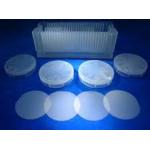
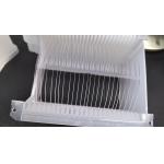
C Plane High Smoothness And High Cleanliness Sapphire Substrate For Semiconductor Sapphire wafers are mainly suitable for the research and development ...
2024-12-09 21:35:54
|
|
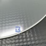
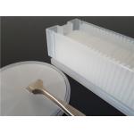
...Wafers Used In Semiconductor, Optical, Medical, Military, Photonic Industry BonTek can make transparent glass wafers from any available glass brand...
2025-07-30 00:13:57
|
|
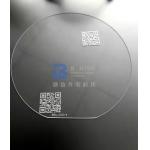
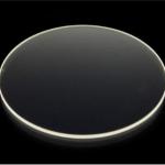
... technology, precision and reliability are non-negotiable. Introducing our premium Fused Silica Wafers – the cornerstone of innovation for high...
2025-04-22 07:45:03
|
|
...Wafer for Semiconductor and MEMS Applications The piezoelectric effect in a crystal is explained as that there will be the development of electric ...
2025-07-30 00:13:57
|
|
...Wafer The Ultimate Choice for Precision Optics and Semiconductors Elevate your technological pursuits with Borofloat® 33 Glass Wafers – the ...
2024-12-10 00:26:38
|
|
...Semiconductor Devices LEDs and High-Temperature Electronics with Sapphire Wafers The Ultimate Solution for High-Performance Applications Unlock ...
2025-04-21 22:24:41
|
|
... Silica Wafer for High-Performance Semiconductor Device Production In the realm of advanced materials, our fused silica wafers shine as a ...
2025-05-30 07:58:46
|
|
... wafers this is the Kyropoulos method (abbreviated to Ky or Kr). The Kyropoulos method is a continuation of the Czochralski method (CZ) which is ...
2024-12-09 20:34:25
|
|
...silicon dioxide (quartz, sand). It lacks long range order in its atomic structure. Its highly cross-linked three-dimensional structure gives rise ...
2025-07-30 00:13:57
|

|
... properties and thermal stability. It is widely used in various industries, including optics, lasers, semiconductors, and scientific research. JGS1 ...
2025-07-30 00:13:57
|