
81 - 90 of 396
semiconductor piezoelectric wafer
Selling leads
|
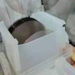
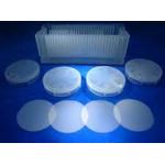
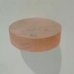
Customized 6 Inch 8 Inch Piezoelectric Wafer for Semiconductor POI and MEMS Positive piezoelectric effect (direct piezoelectric effect) : The ...
2026-03-27 20:05:03
|
|
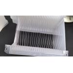
...Piezoelectric Wafer For Piezoelectric Sensor and Transducer With the Piezoelectric Effect the most unique trait of this effect is that it works two ...
2026-03-27 20:05:03
|
|
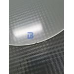
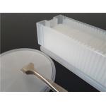
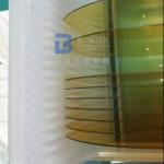
... applications. Crafted from the purest fused silica, our wafers offer unparalleled optical clarity, thermal stability, and chemical resistance. ...
2026-03-27 20:05:03
|
|
...Semiconductor Processes with Fused Silica Wafers Unrivaled Thermal Stability and for Optics and Photonics Our Fused Silica Wafers are crafted from ...
2026-03-27 20:05:03
|
|
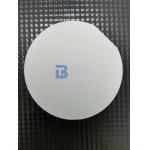
C Plane High Smoothness And High Cleanliness Sapphire Substrate For Semiconductor Sapphire wafers are mainly suitable for the research and development ...
2026-03-27 20:05:03
|
|
...Wafer The Ultimate Choice for Precision Optics and Semiconductors Elevate your technological pursuits with Borofloat® 33 Glass Wafers – the ...
2026-03-27 20:05:03
|
|
...Semiconductor Devices LEDs and High-Temperature Electronics with Sapphire Wafers The Ultimate Solution for High-Performance Applications Unlock ...
2026-03-27 20:05:03
|
|
... Silica Wafer for High-Performance Semiconductor Device Production In the realm of advanced materials, our fused silica wafers shine as a ...
2026-03-27 20:05:03
|
|
... lithium tantalate wafer offers unparalleled piezoelectric, optical, and electro-optic properties, setting it apart from traditional materials. The ...
2026-03-27 20:05:03
|
|
...piezoelectric materials. Developed by our team of experts, these wafers are made from Langasite Crystal and have superior performance compared to ...
2026-03-27 20:05:03
|