
311 - 320 of 396
semiconductor piezoelectric wafer
Selling leads
|
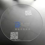
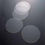
...Wafers Thickness 0.35±0.025mm in Fused Silica Borosilicate BonTek is a recognized participant in the manufacture of transparent Glass wafers. Many ...
2026-03-27 20:05:03
|
|
...Wafer for Consistent Optical Properties C-plane 0001 the Sapphire Wafer - a Unique Innovation in High-Tech Materials Step into the future with our ...
2026-03-27 20:05:03
|
|
...Wafer for SAW Components Unleash the Power of Monocrystalline Quartz Wafers for Your Cutting-Edge Applications! Discover the ultimate material for ...
2026-07-06 00:24:42
|
|
Piezoelectric LiNbO3 Substrate 128Y Cut with Orientation Flat or Notch Lithium Niobate (LiNbO3) is colorless transparent crystal. It belongs to ...
2026-07-06 00:24:42
|
|
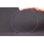
6 Inch And 8 Inch Borofloat 33 Wafer For Electronics Optics And Semiconductors Borofloat 33 Features Schott Borofloat 33 is a flat glass that sets new ...
2026-03-27 20:05:03
|
|
X-cut Y-cut Crystal Quartz Ring Double Side Lapped for Sensing Technology Piezo Quartz exhibits the best long term stability of any piezoelectric ...
2026-07-06 00:24:42
|
|
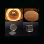
2Inch-6 Inch LED Grade Sapphire Crystal Substrate Sapphire (molecular formula Al2O3) single crystal is an excellent multifunctional material. It has ...
2026-03-27 20:05:03
|
|
... in the semiconductor industries. A common application is the mechanical stabilization of thin Si-diaphragms for sensors, and etching structuring ...
2026-03-27 20:05:03
|
|
... coefficient of thermal expansion. It has a wide range of uses including optical components, semiconductor wafers and microelectronic components. ...
2026-03-27 20:05:03
|
|
...renowned for its exceptional physical and optical properties, forms the cornerstone of our state-of-the-art wafers, designed to meet the most ...
2026-07-06 00:24:42
|