
LED Grade Sapphire Substrate Single Crystal Wafer 2 Inch - 6 Inch
|
|
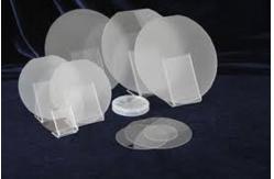
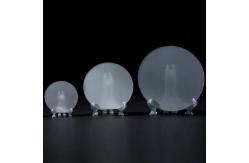
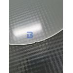
2Inch-6 Inch LED Grade Sapphire Crystal Substrate
Sapphire (molecular formula Al2O3) single crystal is an excellent multifunctional material. It has high temperature resistance, good heat conduction, high hardness, infrared penetration and good chemical stability. Widely used in industry, national defense and scientific research in many fields (such as high temperature resistant infrared window, etc.). At the same time, it is also a kind of single crystal substrate material with a wide range of uses. It is the preferred substrate in the blue, purple, white light emitting diode (LED) and blue laser (LD) industry at present (gallium nitride film needs to be epitaxed on the sapphire substrate first), as well as an important superconducting thin film substrate.
|
||||||||||||||||||||||||||
| Product Tags: Sapphire Substrate Single Crystal Wafer LED Grade Sapphire Wafer 6 Inch Single Crystal Sapphire Wafer |
|
Maximize Your Projects with Borofloat 33 Glass Wafers The Ideal Material for Chemical Sensors and Laboratory Equipment |
|
Experience Unmatched Performance with Single Crystal Quartz Piezoelectric Wafers for Quartz Crystal Oscillators |
|
Upgrade Your Semiconductor Processes with Fused Silica Wafers Unrivaled Thermal Stability and for Optics and Photonics |
|
Upgrade Your Systems with Our Piezoelectric Wafer Endcaps for Precision Engineering and High-Temperature Applications |
|
Stoichiometric LiTaO3 Wafers The Ultimate Solution for High-Performance Optoelectronic and Acoustic Applications |
|
High-Sensitivity Signal Processing with Our Precision Stoichiometric LiNbO3 Piezoelectric Wafer for Optoelectronic Applications |