
1 - 10 of 89
semiconductor fused silica wafer
Selling leads
|
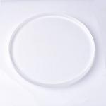
...Fused Silica Wafer for Semiconductor Manufacturing our Fused Silica Wafers, the epitome of precision and performance for cutting-edge applications ...
2025-03-06 16:30:59
|
|
... technology, precision and reliability are non-negotiable. Introducing our premium Fused Silica Wafers – the cornerstone of innovation for high...
2025-04-22 07:45:03
|
|
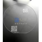
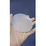
Semiconductor use Fused Silica Wafer with Low CTE for UV Lithography Wafers from semiconductor grade quartz (amorphous) are used in semiconductor ...
2024-12-09 20:34:25
|
|
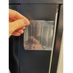
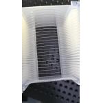
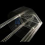
...Fused Silica Wafer Borosilicate Customized Thickness with Flat or Notch Edge ground BonTek works a lot with fused silica, fused quartz, borosilicat...
2024-12-09 20:34:25
|
|
...Fused Silica Wafer and BF33 C7980 BK7 H-K9L Glass Wafers The glass wafers are widely used as bonding material with silicon wafers in semiconductor ...
2024-12-09 20:34:25
|
|
... applications. Crafted from the purest fused silica, our wafers offer unparalleled optical clarity, thermal stability, and chemical resistance. ...
2024-12-10 00:15:50
|
|
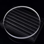
...Fused Silica Wafers Corning 7980 in stock for Immediate Shipment High quality 4 inch SiO2 Fused Silica wafers are in stock for immediate shipment. ...
2024-12-09 20:34:25
|
|
..., the melting method Synthetic CVD. Fused silica is highly heat resist and has a broad transmission range (>85% @185nm, >90% from 200nmto 2000nm). ...
2024-12-09 20:34:25
|
|
...Fused Silica Wafer 4'' 6'' 500um SiO2 HPFS with Excellent Chemical Resistance Fused Silica (SiO2) wafers are made from high purity fused silica, ...
2024-12-09 20:34:25
|
|
... applications requiring unmatched optical clarity and thermal stability. Crafted from high-purity silica glass through a meticulous fusion process, ...
2024-12-10 00:44:27
|