
261 - 270 of 302
saw devices optical wafer
Selling leads
|
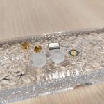
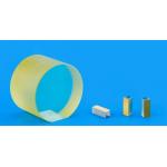
X-cut Y-cut Crystal Quartz Ring IEEE standard Double Side Lapped for Pressure Sensor There are a variety of piezoelectric materials that can conduct ...
2025-07-26 00:13:55
|
|
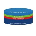
Enabling High-Speed Modulation And Wide Bandwidth With LNOI POI Piezo on Insulation (POI) refers to a technology where piezoelectric materials are ...
2025-07-26 00:13:55
|
|
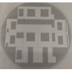
Revolutionizing Chip Fabrication Precision Innovation and Excellence At the forefront of advanced chip foundry services, we empower innovation by ...
2025-04-21 22:24:41
|
|
ZnO crystal substrate is used in GaN(blue LED) epitaxial substrate wide band connection devices and other fields Zinc oxide (ZnO) crystal substrate is ...
2024-12-10 00:32:09
|
|
Unleash the Full Potential of Your Optoelectronic Devices with Our High Thermal Conductivity MgO Single Crystal Substrate Introducing our premium MgO ...
2025-06-28 00:24:28
|
|
...wafers are the epitome of modern semiconductor technology, renowned for their exceptional hardness, chemical stability, and optical transparency. ...
2024-12-09 21:17:37
|
|
..., offer a unique combination of piezoelectric, pyroelectric, and optical properties, making them indispensable for modern electronics. LiTaO3 ...
2024-12-09 22:59:53
|

|
...ultimate solution for enhancing the performance and reliability of your optical and electronic devices. Crafted from high-purity quartz, renowned ...
2024-12-10 00:36:40
|
|
...ultimate solution for enhancing the performance and reliability of your optical and electronic devices. Crafted from high-purity quartz, renowned ...
2025-03-06 16:31:07
|
|
.... It is highly polished with an excellent parallelism of 3 Arc Sec and perpendicularity of 5 Arc Sec. It has great optical properties with a ...
2024-12-09 22:58:07
|