
111 - 120 of 127
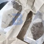
polished transparent sapphire wafer
Selling leads
|
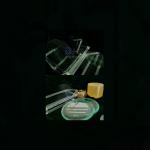
X-cut and Z-cut LiNbO3 wafer 8 inch Large Size For Optical Use Lithium niobate is transparent between 0.25 and 5.3 μm. It can be used in visible, near ...
2025-07-30 00:13:57
|
|
Ra Roughness 1nm LiNbO3 Wafer used in Visible, Near-Infrared and Mid-Infrared Regions Lithium niobate is transparent between 0.25 and 5.3 μm. It can ...
2025-07-30 00:13:57
|
|
Piezoelectric Lithium Niobate Wafer For SAW Interdigital Transducer Making Lithium niobate is transparent between 0.25 and 5.3 μm. It can be used in ...
2024-12-09 21:18:24
|
|
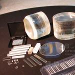
BonTek LiNbO3 Crystal Piezoelectric Wafer 3 inch 4 inch Surface Acoustic Wave With its large electro-optic coefficients, wide optical transparency ...
2025-07-30 00:13:57
|

|
... stability. It is widely used in various industries, including optics, lasers, semiconductors, and scientific research. JGS1 is specifically ...
2025-07-30 00:13:57
|

|
... Piezoelectric Wafer for High-Temperature Superconducting YBCO and More our state-of-the-art LaSrAlO4 crystals, a game-changer in the realm of high...
2024-12-10 00:36:40
|
|
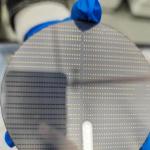
Epi polished Optical grade crystla quartz Wafers for DUV-photolithography Laser Optics Optical grade crystal quartz is used for production of high...
2024-12-09 20:34:25
|
|
6inch 0.5mm LiNbO3 Lithium Niobate Wafer 64Y 128Y Single Side Polished For SAW Device Lithium Niobate has good nonlinear optical properties and can be ...
2024-12-09 20:34:25
|
|
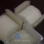
Single Crystal Quartz Cut Into Wafer With Different Orientation Piezo quartz is the highly symmetric shape of the single crystal, is characterized by ...
2024-12-09 21:03:49
|
|
10mm Square SrTiO3 Crystal Wafer For Semiconductor SrTiO3 single crystal has the good lattice structure of perovskite structure materials. For the ...
2024-12-09 21:42:24
|