
Optical Grade Crystla Quartz Wafer
|
|
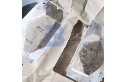
Epi polished Optical grade crystla quartz Wafers for DUV-photolithography Laser Optics
Optical grade crystal quartz is used for production of high-power laser optics and precision polarizing optics such as waveplates and polarization rotators. For these applications most important parameters are the following: refractive index homogeneity, bubbliness category, UV stability, high transmission at DUV range (very important for the purposes of DUV-photolithography), purity and polarization uniformity of the material. To achieve the highest quality this material is grown on one side of the seed through special mask with very slow growth speed. Growth direction is Z-axis (so called Z-cut material)
BonTek Optoelectronics provides high quality Single Crystal Quartz wafers in both SAW grade and optical grade. We can offer various orientation options including X cut, Y cut, Z cut, AT cut, ST cut, etc. or just any cut angle you can imaging for your unique applications at reasonable price. Specially, we can fabricate very LARGE and THIN wafers conform to SEMI-std. 3" 4" 6" 8" are all available as per requirement, and we can polish to 75um for 4" quartz wafers.
FAQs:
A: We look at ourselves as the piezo wafer specialist. We are the very first to work with Single Crystal Quartz in China about 30 years ago. Then gradually we step in the field of LiNbO3, LiTaO3, Quartz glass, LGS, CTGS etc. Especially, if you are looking for a piezo quartz supplier, we are the ultimate choice! We export millions of quartz blanks each year because we master the AT, SC and IT cuts with superior angle precision.
A: Yes, of course. We can fabricate as per your request. In addition, we are so experienced with piezo wafers that we can provide you relevant suggestions if you are not 100% sure about your choice. Besides, we do have some standard wafers in stock, please check with us.
A: Yes, we would suggest you go with the courier agent you are most familiar with (DHL, FedEX, UPS etc.). We can ship via your account. And, of course, we will pack the products safely in acceptable size to help you save the shipping cost. If you need us to take care of the freight, it’s also not a problem. We also have good discount with the international courier companies.
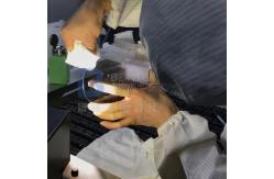
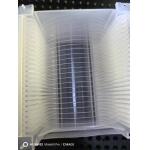
A: The wafer products are fragile and sometimes expensive. The last thing, as the manufacturer, we want to see is the products we make were damaged during courier. As a result, we will pack the wafers adequately and put them in a proper carton filled with buffer sponge. However, accidents are inevitable sometimes. So, please follow the “Acceptance check” steps shown in the drawings below. If the unwanted happened, we will either give the replenishment or refund if you follow the checking steps.
A: Sure. Factory inspection is important for large quantity purchase and long-term cooperation. Face to face discussion is what we mostly confident with. During the past years, big names around the world have witnessed our progress in factory build-up. These days, due to the Covid-19 pandemic, we also had the experience of videoconferencing with global buyers.
Acceptance Check
|
||||||||||||||||||||||||||||||||||||||||||||||||||||||||||||||||||||||||||||||||||||||||||||||||||||||||||||||
| Product Tags: Epi polished crystla quartz Wafers Optics 6 inch Wafer crystla quartz Wafers | ||||||||||||||||||||||||||||||||||||||||||||||||||||||||||||||||||||||||||||||||||||||||||||||||||||||||||||||

|
Monocrystalline Quartz Wafers The Ultimate Material for Your Most Demanding Applications |
|
Single Crystal Quartz Ring With Low Inclusion Density For Pressure Sensing |
|
Highly Accurate Single Crystal Quartz Wafer For TCXO And VCXO Applications |
|
Double Side Polished Single Crystal Quartz Wafer for SAW Components |
|
3 Inch and 4 Inch Single Crystal Quartz Wafer for SAW and MEMS Devices Production Process |
|
X / Y Cut Single Crystal Quartz Ring For Pressure Sensing Thickness Shear |