
41 - 50 of 175
polish quartz wafers
Selling leads
|
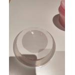
...Polished Sapphire Wafers Sapphire Substrates Specification: Single crystal Al2O3 99.999% Orientation: R-axis 0.5° Diameter:50.8±0.1mm Thickness ...
2024-12-09 21:21:54
|
|
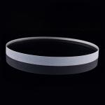
6'' Single Side Polish LiTaO3 Wafer for Nonlinear Optics, Passive Infrared (IR) Sensors The LiTaO3 Lithium Tantalate crystal has >99.99% purity. Find ...
2024-12-09 20:34:25
|
|
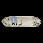
...Polish LiTaO3 Wafer 36Y 42Y For SAW and BAW Applications Lithium Tantalate (LiTaO3) is an ideal material for both SAW and optical use. It has ...
2024-12-09 20:34:25
|
|
Various Type of Glass Wafers Used In Semiconductor, Optical, Medical, Military, Photonic Industry BonTek can make transparent glass wafers from any ...
2025-07-25 00:18:38
|
|
... or wafer made from a thin layer of LiNbO3 material. Size: The thin film has a diameter of 3 inches, which is equivalent to approximately 76 ...
2024-12-09 22:36:19
|
|
...pressure vessel in thermal jacket and heating coils. The first step is to add crushed feeding quartz and filling the vessel with NaOH solution. The ...
2024-12-09 20:34:25
|
|
... in the VIS and UV is approx. The transmission range of significantly cheaper JGS2 wafers is shifted towards longer wavelengths when compared with ...
2024-12-09 20:34:25
|
|
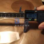
.... If the seed area is not avoided inside the wafer, then it’s "with seed", if we can avoid the seed inside the wafers, then it’s "seedless". The ...
2025-07-25 00:18:38
|
|
... and the reverse effect can also happen. Piezoelectric materials have non-conductive nature and they can be classified as ceramics and crystals. ...
2024-12-09 20:34:25
|
|
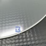
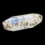
Different Angle Cuts of Single Crystal Quartz Customized Wafers used in various applications BonTek Optoelectronics provides high quality Single ...
2025-07-25 00:18:38
|