
91 - 100 of 341
piezoelectric lithium niobate wafer
Selling leads
|
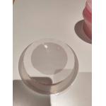
... or wafer made from a thin layer of LiNbO3 material. Size: The thin film has a diameter of 3 inches, which is equivalent to approximately 76 ...
2024-12-09 22:36:19
|
|
...low propagation loss, which can be used to fabricate SAW devices with up to 50% bandwidth. The acoustic surface wave properties of lithium niobate ...
2025-07-14 00:17:42
|

|
..., density of 4.64×10^3kg/m3, Mohs hardness of 5~5.5, melting point of 1253℃, Curie temperature at 1210℃. Lithium niobate single crystal is a kind ...
2025-07-14 00:17:42
|
|
... lithium tantalate wafer offers unparalleled piezoelectric, optical, and electro-optic properties, setting it apart from traditional materials. The ...
2024-12-09 23:27:58
|
|
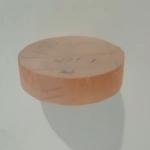
3'' 0.5mm SSP LiTaO3 Wafer X-112Y cut with piezoelectric and pyroelectric properties The piezoelectric and pyroelectric properties of Lithium ...
2025-07-14 00:17:42
|
|
...Wafer Polished 0.25mol% Er Dope Or 5mol% MgO Dope For Optical Applications Doped LN Wafers: Er:LN, MgO:LN, and Fe:LN Doping lithium niobate (LN) ...
2025-07-14 00:17:42
|
|
...Piezoelectric Wafer For Piezoelectric Sensor and Transducer With the Piezoelectric Effect the most unique trait of this effect is that it works two ...
2024-12-09 20:34:25
|
|
... are made from high-purity lithium niobate crystals and offer several advantages due to their larger size. Here is a description of 8-inch LiNbO3 ...
2024-12-09 22:36:19
|
|
...Piezoelectric Crystal Wafer for Semiconductor and MEMS Applications The piezoelectric effect in a crystal is explained as that there will be the ...
2025-07-14 00:17:42
|
|
...Wafer Polished 5mol% MgO Dope For Magnetic and Optical Applications Elevating Performance in Optical & Electronic Applications Experience the next ...
2025-07-14 00:17:42
|