
21 - 30 of 371
optoelectronic applications piezoelectric wafer
Selling leads
|
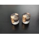
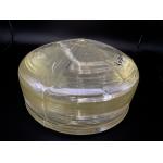
...Piezoelectric Wafer for Accurate Pressure Measurements the Premier Piezoelectric Quartz End Cap Step into the future of precision instrumentation ...
2024-12-09 23:45:42
|
|
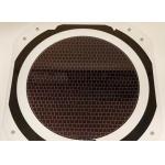
...Piezoelectric Wafer for Higher Frequency SAW devices Free-pyro black LiNbO3 and LiTaO3 wafers were prepared successfully by chemical reduction ...
2024-12-09 20:34:25
|
|
... in these crystals aren’t symmetrical but they still exist in an electrically neutral balance. However, if you apply mechanical pressure to a ...
2025-07-21 00:21:29
|

|
...Piezoelectric Wafer with Designed Cut Angles and Thickness A piezoelectric material is a crystal that has the ability to generate electricity when ...
2024-12-09 20:34:25
|
|
... response in electrical simulation is called the opposite of the piezoelectric effect. In crystalline materials, the number of electrical dipoles ...
2024-12-09 20:34:25
|
|
... effect is classified as piezoelectedric crystal. When electricity is applied to the crystal, an electrical dipole appears to form due to dipoles ...
2025-07-21 00:21:29
|
|
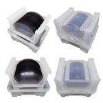
...Piezoelectric Wafers We specialize in providing comprehensive chip foundry services, catering to clients who require high-quality wafer processing ...
2025-04-21 22:24:42
|
|
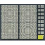
...Piezoelectric Wafer Fabrication for MEMS and SAW Devices Advanced Processing Capabilities for Results We specialize in providing comprehensive chip ...
2025-04-22 07:45:03
|
|
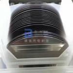
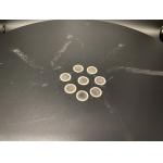
...Piezoelectric Wafers for SAW and MEMS Devices In the dynamic fields of electronics, telecommunications, and sensors, the demand for high - quality ...
2025-06-28 00:24:28
|
|
...Wafer is a type of semiconductor material made of sapphire, which has excellent optical, mechanical, and chemical properties. It is commonly used ...
2024-12-09 23:27:58
|