
271 - 280 of 378
optoelectronic applications piezoelectric wafer
Selling leads
|
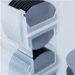
...Wafer 4'' 6'' 8'' for MEMS Devices Glass wafers made of borosilicate glass are often used in Semiconductor and MEMS industry in a wide variety of ...
2024-12-09 20:34:25
|
|
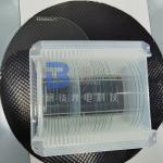
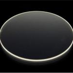
Piezoelectric LiNbO3 Substrate 128Y Cut with Orientation Flat or Notch Lithium Niobate (LiNbO3) is colorless transparent crystal. It belongs to ...
2025-07-29 00:13:51
|
|
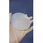
2Inch-6 Inch LED Grade Sapphire Crystal Substrate Sapphire (molecular formula Al2O3) single crystal is an excellent multifunctional material. It has ...
2024-12-09 21:35:54
|
|
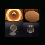
...Wafer Polished 5mol% MgO Dope For Magnetic and Optical Applications Elevating Performance in Optical & Electronic Applications Experience the next ...
2025-07-29 00:13:51
|

|
... AG, a leading glass manufacturer. B270 glass wafer is known for its high optical quality, flatness, and versatility, making it suitable for a wide ...
2025-07-29 00:13:51
|
|
...Wafer for Surface Acoustic Wave IDT Applications Free-pyro black LiNbO3 and LiTaO3 wafers were prepared successfully by chemical reduction under a ...
2024-12-09 20:34:25
|
|
... wafers this is the Kyropoulos method (abbreviated to Ky or Kr). The Kyropoulos method is a continuation of the Czochralski method (CZ) which is ...
2024-12-09 20:34:25
|

|
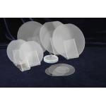
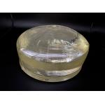
...Wafers The Ultimate Material for Your Most Demanding Applications the power of innovation with our premium Quartz Wafers, the cornerstone of ...
2025-07-29 00:13:51
|
|
... applications requiring unmatched optical clarity and thermal stability. Crafted from high-purity silica glass through a meticulous fusion process, ...
2024-12-10 00:44:27
|
|
... coupling coefficient and low acoustic attenuation. Typical cut angle for SAW application is 36°Y, 42°Y, X-cut etc. The Lithium Tantalate reduction ...
2024-12-09 20:34:25
|