
151 - 160 of 247
optical doped wafer
Selling leads
|
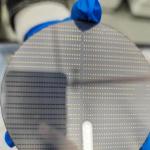
...Wafer used in Visible, Near-Infrared and Mid-Infrared Regions Lithium niobate is transparent between 0.25 and 5.3 μm. It can be used in visible, ...
2024-12-09 20:34:25
|
|
... in both electro-optic and acousto-optic fields. These can be: surface acoustic devices, bulk acoustic devices, piezoelectric transducers and ...
2024-12-09 20:34:25
|
|
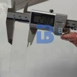
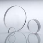
Z-Cut X-Cut LiNbO3 Crystals Wafer Optical Grade Both Sides Polish The sound velocity for the longitudinal waves in LiNbO3 propagating along the ...
2025-07-31 00:19:35
|
|
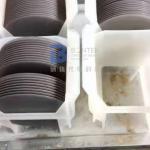
Piezoelectric Crystal Lithium Tantalate Wafer LT LiTaO3 Crystals Lithium Tantalate (LT, LiTaO3) has unique properties. It is used in Electro-Optical ...
2025-07-31 00:19:35
|
|
...ferroelectric, lithium niobate demonstrates piezoelectric effect, nonlinear optic effects, photoelastic effect and Pockels effect (linear electro...
2024-12-09 21:18:24
|
|
High Resistance Sapphire Polished Wafer 3 Inch C-Plane Optical Crystal Sapphire is a single crystal of alumina and is the second-hardest material in ...
2024-12-09 21:35:54
|
|
...le having a very broad transmission range. Applications include: · Windows - FLIR (Forward Looking Infra Red) windows for sensors and other optics. ...
2024-12-09 21:35:54
|
|
..., and beyond. This unique crystalline compound boasts an exceptional combination of properties, making it a cornerstone in modern technology. ...
2024-12-10 00:15:50
|
|
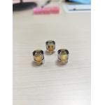
...Wafer Endcaps for Precision Engineering and High-Temperature Applications Enhance the efficiency and reliability of your optical assemblies with ...
2025-07-24 13:36:24
|
|
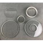
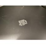
Revolutionize Your Optical Applications with Piezoelectric Wafer Quartz Rings Discover the pinnacle of sensor technology with our Piezoelectric Quartz ...
2025-07-26 00:13:26
|