
61 - 70 of 321
lithography etching piezoelectric wafers
Selling leads
|
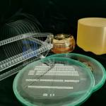
Customized 6 Inch 8 Inch Piezoelectric Wafer for Semiconductor POI and MEMS Positive piezoelectric effect (direct piezoelectric effect) : The ...
2024-12-09 20:34:25
|
|
... that have this property fall under the category "piezoelectric." Mechanical or electrical energy can be applied to the same piezoelectedrical ...
2024-12-09 20:34:25
|
|
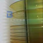
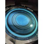
...-frequency microwave applications and piezoelectric devices. Crafted from lithium tantalate (LiTaO3), a material renowned for its exceptional ...
2024-12-10 00:44:27
|
|
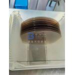
... Your Technology with LGS Wafer: A Reliable Solution for Diverse Applications Product Description: Langasite Wafers LGS piezoelectric wafers, also ...
2024-12-09 23:27:58
|
|
... devices. Crafted from high-quality Lithium Niobate (LiNbO3), these wafers offer an exceptional combination of optical, ferroelectric, and ...
2024-12-10 00:31:18
|
|
...Wafers The Ultimate Solution for Piezoelectric Applications the precision-engineered heart of advanced technology. These wafers, crafted from the ...
2025-08-03 00:13:22
|
|
...Wafers The Superior Choice for High-Frequency Microwave Applications and Piezoelectric Devices our premium LiTaO3 Wafers, the epitome of cutting...
2025-03-06 16:31:01
|
|
Customized 6 Inch 8 Inch Piezoelectric Wafer for POI Applications and MEMS Piezoelectric effect is defined as the change in electric polarization of ...
2024-12-09 20:34:25
|
|
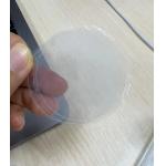
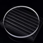
Semiconductor use Fused Silica Wafer with Low CTE for UV Lithography Wafers from semiconductor grade quartz (amorphous) are used in semiconductor ...
2024-12-09 20:34:25
|
|
... is subjected to mechanical stress, an electric field or charge proportional to the stress will be generated. This phenomenon is called the ...
2024-12-09 20:57:43
|