
101 - 110 of 311
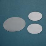
lithography etching piezoelectric wafers
Selling leads
|
... applications are surface acoustic wave devices, bulk acoustic wave devices, piezo-electric transducers, pyroelectric infrared sensor and ...
2025-07-15 00:17:51
|
|
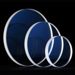
...ferroelectric, lithium niobate demonstrates piezoelectric effect, nonlinear optic effects, photoelastic effect and Pockels effect (linear electro...
2024-12-09 21:18:24
|
|
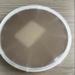
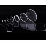
...LiTaO3) wafer is used for several optical devices, especially surface acoustic wave(SAW) device. Because of the lithography in SAW device process, ...
2024-12-09 20:34:25
|
|
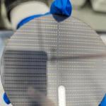
...Wafer used for Optical Devices, SAW Devices Compound semiconductors are the semiconductors composed of more than two chemical elements. Lithium ...
2025-07-15 00:17:51
|
|
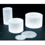
High-Performance Sapphire Wafer with Perpendicularity ≤3 Arc Min for Industrial Applications Product Description: Sapphire Slice, Sapphire Wafer, ...
2024-12-09 23:10:26
|
|
Superior Quality Sapphire Wafer ≤3μm TTV Roundness Edge Grinding Product Description: Sapphire Wafer is an advanced substrate made of sapphire ...
2024-12-09 23:10:26
|
|
2Inch 3Inch 4Inch Sapphire Wafer for Miniature Electronic Devices the Sapphire Crystal Wafer - a cutting-edge material that revolutionizes optical, ...
2024-12-09 23:27:58
|
|
C-plane 0001 Orientation C-plane Sapphire Wafer with A-plane 11-20 Primary Flat Unlock the full potential of your semiconductor, LED, and optical ...
2024-12-10 00:26:38
|
|
High-Capacity Holographic Information Solution Stoichiometric LiTaO3 Wafer Lstoichiometric LiTaO3 wafers, the epitome of precision and performance for ...
2024-12-10 00:26:38
|
|
Thermal Conductivity C-plane 0001 Sapphire Wafer Al2O3 Substrate for Infrared Window Sapphire Wafers, the cornerstone of advanced technology and ...
2025-07-15 00:17:51
|