
261 - 270 of 311
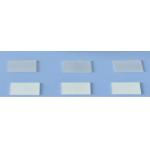
lithography etching piezoelectric wafers
Selling leads

|
Revolutionize Your Technology with Premium Strontium Titanate (SrTiO₃) Crystals Strontium Titanate (SrTiO₃) crystals, a revolutionary material at the ...
2024-12-10 00:36:40
|
|
|
ZnO Crystal Substrate Is Used In GaN(blue LED) Epitaxial Substrate Wide Band Connection Devices And Other Fields the cutting-edge of material science ...
2024-12-10 00:36:40
|
|
ZnO Crystal Substrate Ideal Material for High Temperature/High Energy Electronic Devices and Future Wireless Communication our state-of-the-art ZnO ...
2024-12-10 00:44:27
|
|
High Purity ZnO Crystal Substrate for UV Optoelectronics and Energy Harvesting Solutions Discover the remarkable qualities of ZnO Crystal, a versatile ...
2025-03-06 16:31:06
|
|
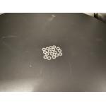
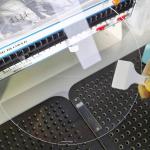
Optimal Performance Single Crystal Quartz Ring for Specific Customer Requirements Elevate your precision instrumentation and optical applications with ...
2025-03-07 07:43:38
|
|
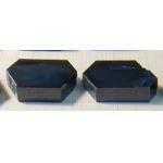
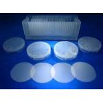
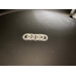
C Plane High Smoothness And High Cleanliness Sapphire Substrate For Semiconductor Sapphire wafers are mainly suitable for the research and development ...
2024-12-09 21:35:54
|
|
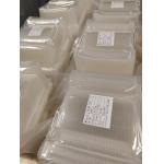
Highly Polished Sapphire Slice 0.5mm-3mm Thickness 2inch-8inch Diameter Product Description: Sapphire Wafer is a kind of high precision sapphire ...
2024-12-09 23:10:26
|
|
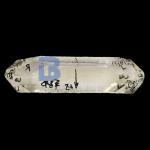
Single Crystal Quartz Wafer for High-Performance Pressure Sensing Solutions Single Crystal Quartz Rings Elevate your scientific, industrial, or ...
2025-07-16 00:18:07
|
|
Borofloat 33 Glass Substrate The Ultimate Solution for High-Tech Applications Requiring Unmatched Performance Are you in search of a high - performanc...
2025-05-30 07:58:46
|
|
.... If the seed area is not avoided inside the wafer, then it’s "with seed", if we can avoid the seed inside the wafers, then it’s "seedless". The ...
2025-07-16 00:18:07
|