
111 - 120 of 177
lithium tantalate polishing wafer
Selling leads
|
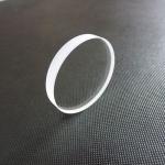
Fe doped Lithium Niobate Wafer Optical Grade and SAW Grade Lithium Niobate (LiNbO3) is a useful optoelectronic material. The material not only has ...
2025-07-16 00:18:07
|
|
...Wafer used in Visible, Near-Infrared and Mid-Infrared Regions Lithium niobate is transparent between 0.25 and 5.3 μm. It can be used in visible, ...
2025-07-16 00:18:07
|
|
... and the reverse effect can also happen. Piezoelectric materials have non-conductive nature and they can be classified as ceramics and crystals. ...
2024-12-09 20:34:25
|
|
... stress, an electric field or charge proportional to the stress will be generated. This phenomenon is called the positive piezoelectric effect. ...
2024-12-09 20:57:43
|
|
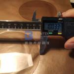
.... It has an orientation of ±0.5°, a wafer shape, a clear aperture of greater than 90%, and TTV of ≤3μm. It is also customizable in size to meet the ...
2024-12-09 23:10:26
|
|
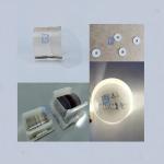
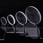
Diameter 6inch Sapphire Wafer LED Grade Polished Transparent Product Description: Sapphire Wafer is a high-precision sapphire substrate with superior ...
2024-12-09 23:10:26
|
|
Diameter 4inch Sapphire Wafer grade with Single Side Polished Surface Quality Product Description: Sapphire Wafer – The Ultimate Sapphire Plate ...
2024-12-09 23:10:26
|
|
...Polished LED Sapphire Wafer with BOW 10um Product Description: Sapphire Wafer is a kind of sapphire slice that has been precision cut from a ...
2024-12-09 23:10:26
|
|
...Wafer and BF33 C7980 BK7 H-K9L Glass Wafers The glass wafers are widely used as bonding material with silicon wafers in semiconductor industry. ...
2024-12-09 20:34:25
|
|
..., chemically etched or polished. The cut angles mostly used are: family of AT-cuts, BT-cut, CT-cut, DT-cut, X-cut and Y-cut. They are used for ...
2025-07-16 00:18:07
|