
71 - 80 of 91
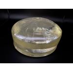
lithium niobate wafer 128y cut
Selling leads

|
... photonic, electronic, and sensing applications. These wafers harness the remarkable properties of LiNbO3, including its strong electro-optic ...
2025-03-06 16:31:02
|
|
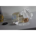
... crystals, LN (lithium niobate) crystal is often the material of choice for optical modulation and Q-switch at near-infrared and infrared ...
2025-07-18 00:17:53
|
|
...Wafers We specialize in providing comprehensive chip foundry services, catering to clients who require high-quality wafer processing and fabricatio...
2025-04-21 22:24:42
|
|
...Wafer Fabrication for MEMS and SAW Devices Advanced Processing Capabilities for Results We specialize in providing comprehensive chip foundry ...
2025-04-22 07:45:03
|
|
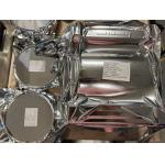
... are made from high-purity lithium niobate crystals and offer several advantages due to their larger size. Here is a description of 8-inch LiNbO3 ...
2024-12-09 22:36:19
|

|
...material engineering, blending the inherent strengths of Lithium Niobate with the enhancing effects of Magnesium Oxide doping. This precise 5% ...
2024-12-10 00:31:18
|
|
...Wafer Polished 5mol% MgO Dope For Magnetic and Optical Applications Elevating Performance in Optical & Electronic Applications Experience the next ...
2025-07-18 00:17:53
|
|
... Piezoelectric Wafer for Optoelectronic Applications Stoichiometric LiNbO₃ Wafers: Precision Engineered for Next-Gen Photonics Unlock unparallele...
2025-05-29 14:33:33
|
|
... or wafer made from a thin layer of LiNbO3 material. Size: The thin film has a diameter of 3 inches, which is equivalent to approximately 76 ...
2024-12-09 22:36:19
|
|
...Wafer 3" 4" for Infrared Wavelength Modulation and Q-Switch Unlock the full potential of your optical and electro-optic systems with LiNbO3 – the ...
2025-07-18 00:17:53
|