
61 - 70 of 153
lithium niobate piezo wafer
Selling leads
|
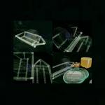
... sensors, optical modulators and various other linear and non-linear optical applications. BonTek is proud to announce that we can provide the ...
2025-07-14 00:17:42
|
|
...low propagation loss, which can be used to fabricate SAW devices with up to 50% bandwidth. The acoustic surface wave properties of lithium niobate ...
2025-07-14 00:17:42
|
|
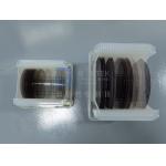
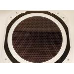
...Wafer 8 Inch 128Y-cut SAW IDT Application Lithium Niobate (LiNbO3) is a ferroelectric material suitable for a variety of applications. Its ...
2025-07-14 00:17:42
|

|
..., density of 4.64×10^3kg/m3, Mohs hardness of 5~5.5, melting point of 1253℃, Curie temperature at 1210℃. Lithium niobate single crystal is a kind ...
2025-07-14 00:17:42
|
|
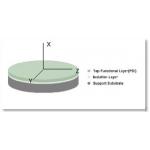
.... LNOI substrates are fabricated by transferring a thin layer of lithium niobate (LiNbO3) crystal onto an insulating substrate, typically silicon ...
2025-07-14 00:17:42
|
|
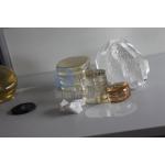
...Wafer Polished 0.25mol% Er Dope Or 5mol% MgO Dope For Optical Applications Doped LN Wafers: Er:LN, MgO:LN, and Fe:LN Doping lithium niobate (LN) ...
2025-07-14 00:17:42
|
|
... Piezoelectric Wafer for Optoelectronic Applications Stoichiometric LiNbO₃ Wafers: Precision Engineered for Next-Gen Photonics Unlock unparallele...
2025-05-29 14:33:33
|
|
...Wafers We specialize in providing comprehensive chip foundry services, catering to clients who require high-quality wafer processing and fabricatio...
2025-04-21 22:24:42
|
|
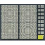
...Wafer Fabrication for MEMS and SAW Devices Advanced Processing Capabilities for Results We specialize in providing comprehensive chip foundry ...
2025-04-22 07:45:03
|
|
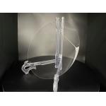
...Wafer for Higher Frequency SAW Devices Piezoelectric Wafer Description The basic principle of SAW devices is the generation of elastic surface ...
2024-12-09 20:34:25
|