
131 - 140 of 243
er ln optical wafer
Selling leads
|
... and H2. Bulk conductivity and optical transmittance of the black LiNbO3 and black LiTaO3 wafers were measured. The results showed that the ...
2024-12-09 20:34:25
|
|
...Wafer for Higher Frequency SAW devices Free-pyro black LiNbO3 and LiTaO3 wafers were prepared successfully by chemical reduction under a mixed ...
2024-12-09 20:34:25
|
|
...Wafer for Surface Acoustic Wave IDT Applications Free-pyro black LiNbO3 and LiTaO3 wafers were prepared successfully by chemical reduction under a ...
2024-12-09 20:34:25
|
|
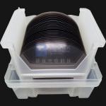
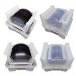
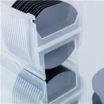
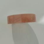
Product Description: 8-inch LiNbO3 wafers refer to the specific size of LiNbO3 crystal substrates commonly used in the fabrication of optoelectronic ...
2024-12-09 22:36:19
|
|
...Wafer for High-Power-Frequency Converters Push the boundaries of technology with our cutting-edge LiTaO3 Wafers. As a premier material for high...
2024-12-10 00:26:38
|
|
... crafted from the purest form of sapphire crystal, renowned for its exceptional hardness, durability, and optical clarity. Designed to withstand ...
2025-07-26 00:13:55
|

|
...Wafer for High-End Microelectronics and Power Devices our premium Sapphire Wafers, the cornerstone of advanced technology and cutting-edge ...
2024-12-10 00:36:40
|

|
...-edge material known for its exceptional piezoelectric, ferroelectric, and optical properties. Ideal for a wide range of advanced applications, SLT ...
2025-03-06 16:31:05
|
|
...Wafer for Semiconductor Manufacturing our Fused Silica Wafers, the epitome of precision and performance for cutting-edge applications in photonics, ...
2025-03-06 16:30:59
|
|
... technology, precision and reliability are non-negotiable. Introducing our premium Fused Silica Wafers – the cornerstone of innovation for high...
2025-04-22 07:45:03
|