
71 - 80 of 151
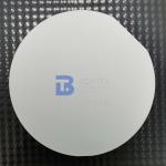
customized thickness litao3 wafer
Selling leads
|
...-optic and photorefractive effects. With the rapidly growing demand for higher information storage capacity, Fe doped Lithium Tantalate (Fe:LiTaO3) ...
2025-07-31 00:19:35
|
|
..., thermal, and mechanical stability, availability of big crystals of sufficiently high quality and, last but not least, its lead-free composition. ...
2025-07-31 00:19:35
|
|
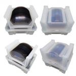
...Wafer As Carrier Wafers Due to their low thickness, thin wafers are vulnerable to stress and breakage. Warping of the wafers during handling and ...
2025-07-31 00:19:35
|
|
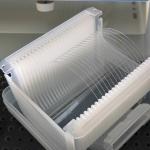
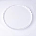
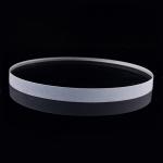
... Wafer Borosilicate Customized Thickness with Flat or Notch Edge ground BonTek works a lot with fused silica, fused quartz, borosilicate, and soda ...
2024-12-09 20:34:25
|
|
...semiconductor industry. Carrier wafers are needed to enable handling and processing of the thin and ultra-thin wafers. Glass and quartz are ...
2024-12-09 20:34:25
|
|
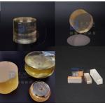
...Customized Fused Silica Wafer and BF33 C7980 BK7 H-K9L Glass Wafers The glass wafers are widely used as bonding material with silicon wafers in ...
2024-12-09 20:34:25
|
|
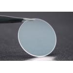
...Wafer Sapphire Wafer 330um 430um Thick Our sapphire wafers are the epitome of precision and quality, crafted from the purest sapphire crystal. ...
2024-12-09 20:34:25
|
|
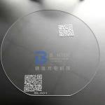
...Wafers Thickness 0.35±0.025mm in Fused Silica Borosilicate BonTek is a recognized participant in the manufacture of transparent Glass wafers. Many ...
2024-12-09 20:34:25
|
|
... in the VIS and UV is approx. The transmission range of significantly cheaper JGS2 wafers is shifted towards longer wavelengths when compared with ...
2024-12-09 20:34:25
|
|
...an ideal material for Anodic bonding. BonTek provides borosilicate wafers from 2 to 14 inches diameter, the thickness is 100um up with low ...
2024-12-09 20:34:25
|