
71 - 80 of 180
customized lithium niobate wafer
Selling leads
|
... is the key to success. Enter our Stoichiometric Lithium Niobate Wafer – a cutting - edge solution that will revolutionize your projects. Crafted ...
2026-03-27 20:05:03
|

|
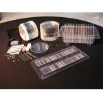
4'' 0.35mm DSP SSP LiNbO3 Wafer 128Y-Cut and 36Y-Cut For SAW Filters Transducers Lithium Niobate is a ferroelectric material suitable for a variety of ...
2026-03-27 20:05:03
|

|
3''- 8'' LiNbO3 Piezoelectric Wafer The Optimal Choice for Frequency Conversion Applications our premium LiNbO3 (Lithium Niobate) crystals, the ...
2026-03-27 20:05:03
|
|
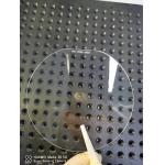
... even if the electric potential occurs instantaneously. The pyroelectric effect of LN wafer is almost eliminated and the transmittance is ...
2026-04-20 00:26:01
|
|
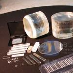
Customized LiNbO3 LiTaO3 Piezo Wafer Optical doped or SAW grade Lithium Niobate has good nonlinear optical properties and can be used as optical ...
2026-03-27 20:05:03
|
|
...wafers of different Orientations For SAW Devices Optical Waveguides Lithium Niobate (LN) is a ferroelectric material with excellent electro-optic, ...
2026-04-20 00:26:01
|
|
...Wafer used in Visible, Near-Infrared and Mid-Infrared Regions Lithium niobate is transparent between 0.25 and 5.3 μm. It can be used in visible, ...
2026-04-20 00:26:01
|
|
...Wafer used in Visible, Near-Infrared and Mid-Infrared Regions Lithium niobate is transparent between 0.25 and 5.3 μm. It can be used in visible, ...
2026-04-20 00:26:01
|
|
... sensors, optical modulators and various other linear and non-linear optical applications. BonTek is proud to announce that we can provide the ...
2026-04-20 00:26:01
|
|
...low propagation loss, which can be used to fabricate SAW devices with up to 50% bandwidth. The acoustic surface wave properties of lithium niobate ...
2026-04-20 00:26:01
|