
11 - 20 of 67
compound semiconductor wafer
Selling leads
|
... applications. Crafted from the purest fused silica, our wafers offer unparalleled optical clarity, thermal stability, and chemical resistance. ...
2024-12-10 00:15:50
|
|
... of people. Silicon comes second as the most common element in the universe; it is mostly used as a semiconductor in the technology and electronic ...
2024-12-09 21:18:07
|
|
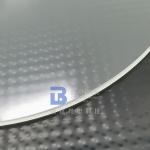
...Wafer For Electronics, Optics, And Semiconductors Borofloat 33 Glass Wafer Description Borofloat 33 is a type of borosilicate glass that is widely ...
2024-12-09 22:13:23
|
|
...Wafer 4'' 6'' 8'' for MEMS Devices Glass wafers made of borosilicate glass are often used in Semiconductor and MEMS industry in a wide variety of ...
2024-12-09 20:34:25
|
|
... coefficient of thermal expansion. It has a wide range of uses including optical components, semiconductor wafers and microelectronic components. ...
2024-12-09 22:58:07
|
|
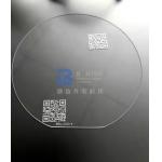
...Wafers Used In Semiconductor, Optical, Medical, Military, Photonic Industry BonTek can make transparent glass wafers from any available glass brand...
2025-07-24 00:21:42
|
|
.... Fused Silica Wafer has very low thermal expansion coefficient, excellent electrical insulation properties, and superior thermal shock resistance. ...
2024-12-09 22:58:07
|
|
... technology, precision and reliability are non-negotiable. Introducing our premium Fused Silica Wafers – the cornerstone of innovation for high...
2025-04-22 07:45:03
|
|
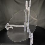
...Wafer for Semiconductor and MEMS Applications The piezoelectric effect in a crystal is explained as that there will be the development of electric ...
2025-07-24 00:21:42
|
|
...Wafer The Ultimate Choice for Precision Optics and Semiconductors Elevate your technological pursuits with Borofloat® 33 Glass Wafers – the ...
2024-12-10 00:26:38
|