
11 - 20 of 58
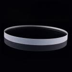
13 fused silica wafer
Selling leads
|
... in the VIS and UV is approx. The transmission range of significantly cheaper JGS2 wafers is shifted towards longer wavelengths when compared with ...
2024-12-09 20:34:25
|
|
...Fused Silica Wafer Borosilicate Customized Thickness with Flat or Notch Edge ground BonTek works a lot with fused silica, fused quartz, borosilicat...
2024-12-09 20:34:25
|
|
...Fused Silica Wafer and BF33 C7980 BK7 H-K9L Glass Wafers The glass wafers are widely used as bonding material with silicon wafers in semiconductor ...
2024-12-09 20:34:25
|
|
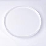
Semiconductor use Fused Silica Wafer with Low CTE for UV Lithography Wafers from semiconductor grade quartz (amorphous) are used in semiconductor ...
2024-12-09 20:34:25
|
|
... optical window material, base plate, etc. Material Brand Schott Borofloat33 / BK7 / B270 / D263 etc. Corning Eagle XG , Fused Silica 7980 /
2025-07-30 00:13:57
|
|
Fused Silica Quartz Borosilicate Glass Wafer As Carrier Wafers Due to their low thickness, thin wafers are vulnerable to stress and breakage. Warping ...
2025-07-30 00:13:57
|
|
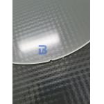
... applications. Crafted from the purest fused silica, our wafers offer unparalleled optical clarity, thermal stability, and chemical resistance. ...
2024-12-10 00:15:50
|
|
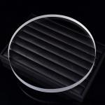
UV grade Fused Silica Wafer customized Diameter Thickness JGS1 JGS2 JGS3 BonTek works on a variety of glass and quartz materials depending on the ...
2025-07-30 00:13:57
|
|
... component must meet the strictest standards. That's where our Fused Silica Wafers shine, offering a level of quality and performance that sets ...
2025-06-28 00:24:28
|
|
...Fused Silica Wafers Unrivaled Thermal Stability and for Optics and Photonics Our Fused Silica Wafers are crafted from ultra-pure, synthetic fused ...
2025-07-24 13:36:24
|