
21 - 30 of 47
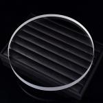
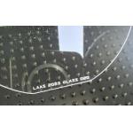
12inch fused silica substrates
Selling leads
|
Semiconductor use Fused Silica Wafer with Low CTE for UV Lithography Wafers from semiconductor grade quartz (amorphous) are used in semiconductor ...
2024-12-09 20:34:25
|
|
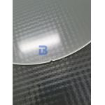
JGS1 JGS2 JGS3 Customized Fused Silica Wafer and BF33 C7980 BK7 H-K9L Glass Wafers The glass wafers are widely used as bonding material with silicon ...
2024-12-09 20:34:25
|
|
... applications. Crafted from the purest fused silica, our wafers offer unparalleled optical clarity, thermal stability, and chemical resistance. ...
2024-12-10 00:15:50
|
|
... Fused Silica Wafers for Advanced Applications our premium Fused Silica, the ultimate material for demanding optical and high-temperature ...
2025-03-06 16:31:00
|
|
... component must meet the strictest standards. That's where our Fused Silica Wafers shine, offering a level of quality and performance that sets ...
2025-06-28 00:24:28
|
|
Upgrade Your Semiconductor Processes with Fused Silica Wafers Unrivaled Thermal Stability and for Optics and Photonics Our Fused Silica Wafers are ...
2025-07-24 13:36:24
|
|
Customizable Fused Silica Wafer for High-Performance Semiconductor Device Production In the realm of advanced materials, our fused silica wafers shine ...
2025-05-30 07:58:46
|
|
4 to 12 inch BF33 Glass Wafers CTE Adapted to Silicon use for Anodic Bonding Borosilicate wafers are of high chemical resistance and thermal stability...
2024-12-09 20:34:25
|
|
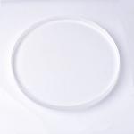
Product Description: Fused Silica Wafer is an optical-grade monocrystalline wafer made of quartz material, also known as fused quartz or fused silica. ...
2024-12-09 22:58:07
|
|
Product Description: Fused Silica Wafer is a kind of Calcium Silicate Board, also known as Glass Wafer. It is a precision engineered and manufactured ...
2024-12-09 22:58:07
|