
1 - 10 of 50
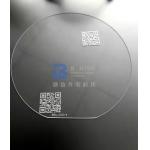
12 inch fused silica wafer
Selling leads
|
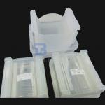
...an ideal material for Anodic bonding. BonTek provides borosilicate wafers from 2 to 14 inches diameter, the thickness is 100um up with low ...
2024-12-09 20:34:25
|
|
...inch 100mm SiO2 Fused Silica Wafers Corning 7980 in stock for Immediate Shipment High quality 4 inch SiO2 Fused Silica wafers are in stock for ...
2024-12-09 20:34:25
|
|
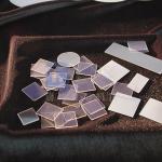
...Fused Silica Wafer JGS3 C7979 and SK1310 with Very Low OH content There are also IR grade Fused Silica wafers with transmission from 185nm to 350nm...
2024-12-09 20:34:25
|

|
...Fused Quartz and Fused Silica Wafer in Infrared and Ultraviolet Spectrum Fused Silica or Fused Quartz which is the amorphous phase of quartz (SiO2)...
2025-07-25 00:18:38
|
|
..., the melting method Synthetic CVD. Fused silica is highly heat resist and has a broad transmission range (>85% @185nm, >90% from 200nmto 2000nm). ...
2024-12-09 20:34:25
|
|
...Fused Silica Wafer 4'' 6'' 500um SiO2 HPFS with Excellent Chemical Resistance Fused Silica (SiO2) wafers are made from high purity fused silica, ...
2024-12-09 20:34:25
|
|
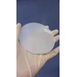
...Fused Silica Wafer for Semiconductor Manufacturing our Fused Silica Wafers, the epitome of precision and performance for cutting-edge applications ...
2025-03-06 16:30:59
|
|
... technology, precision and reliability are non-negotiable. Introducing our premium Fused Silica Wafers – the cornerstone of innovation for high...
2025-04-22 07:45:03
|
|
... applications requiring unmatched optical clarity and thermal stability. Crafted from high-purity silica glass through a meticulous fusion process, ...
2024-12-10 00:44:27
|
|
... CVD. Fused silica is highly heat resist and has a broad transmission range (>85% @185nm, >90% from 200nmto 2000nm). The most seen brand/grade is ...
2025-07-25 00:18:38
|