
61 - 70 of 92
128y cut lithium niobate wafer
Selling leads
|
...Wafer used in Visible, Near-Infrared and Mid-Infrared Regions Lithium niobate is transparent between 0.25 and 5.3 μm. It can be used in visible, ...
2025-08-03 00:13:22
|
|
...Wafer used in Visible, Near-Infrared and Mid-Infrared Regions Lithium niobate is transparent between 0.25 and 5.3 μm. It can be used in visible, ...
2025-08-03 00:13:22
|
|
...Wafer Optical doped or SAW grade Lithium Niobate has good nonlinear optical properties and can be used as optical waveguide material, or to produce ...
2024-12-09 20:34:25
|
|
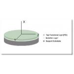
.... LNOI substrates are fabricated by transferring a thin layer of lithium niobate (LiNbO3) crystal onto an insulating substrate, typically silicon ...
2025-08-03 00:13:22
|
|
...Wafer for Higher Frequency SAW Devices Piezoelectric Wafer Description The basic principle of SAW devices is the generation of elastic surface ...
2024-12-09 20:34:25
|
|
...Wafer Polished 0.25mol% Er Dope Or 5mol% MgO Dope For Optical Applications Doped LN Wafers: Er:LN, MgO:LN, and Fe:LN Doping lithium niobate (LN) ...
2025-08-03 00:13:22
|
|
...Wafers The Perfect Choice for Compact and High-Performance Optical Communication Revolutionize Photonics with Ultra-Low-Loss LNOI Wafers Next...
2025-05-29 14:33:33
|
|
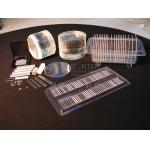
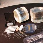
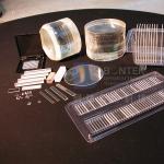
Y128-Cut 4 inch 0.5mm LiNbO3 Wafer DSP pack in Cassette Lithium Niobate (LiNbO3, LNO), an uniaxial ferroelectric with a very high Curie temperature ...
2025-08-03 00:13:22
|

|
... photonic, electronic, and sensing applications. These wafers harness the remarkable properties of LiNbO3, including its strong electro-optic ...
2025-03-06 16:31:02
|
|
... crystals, LN (lithium niobate) crystal is often the material of choice for optical modulation and Q-switch at near-infrared and infrared ...
2025-08-03 00:13:22
|