Designability Flexible Boards PCB Board Design Electronics Device
High - Tg FR4 Prototype PCB Assembly Description: 1. Focus on component sourcing.
2. Management team with 10+ years of experience in the material.
3. PCB Component Sourcing Teams: Project department, Engineering
department, Purchasing.
4. department, Quality department, Customs Declaration department.
5. Professional component validation engineers.
6. Professional BOM Engineers. Prototype PCB Assembly Parameters: | Item | Technical Parameter | | Layer | 2-64 | | Thickness | 0.3-6.5mm | | Copper Thickness | 0.3-12 oz | | Min Mechanical Hole | 0.1mm | | Min Laser Hole | 0.075mm | | HDI | 1+n+1,2+n+2,3+n+3 | | Max Aspect Ratio | 20:01 | | Max Board Size | 650mm*1130mm | | Min Width/Space | 2.4/2.4mil | | Min Outline Tolerance | ±0.1mm | | Impedance Tolerance | ±5% | | Min PP Thickness | 0.06mm | | Bow &Twist | ≤0.5% | | Materials | FR4, High-Tg FR4, Rogers, Nelco, RCC, PTFE, M4, M6, TU862, TU872 | | Surface Finished | HASL, HASL Pb Free Immersion Gold/Tin/Silver Osp, Immersion
Gold+OSP | | Special Capability | Gold Finger Plating, Peelable, Carbon ink |
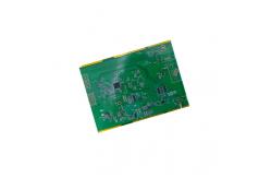
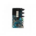
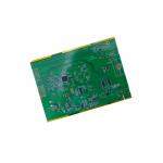
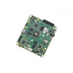
Prototype PCB Assembly Introduction: The design of the printed circuit board is based on the circuit
schematic diagram to realize the functions required by the circuit
designer. The design of the printed circuit board mainly refers to
the layout design, and the layout of external connections needs to
be considered. Various factors such as the optimal layout of
internal electronic components, the optimal layout of metal
connections and vias, electromagnetic protection, heat dissipation,
etc. Excellent layout design can save production costs and achieve
good circuit performance and heat dissipation performance. Simple
layout design can be realized by hand, and complex layout design
needs to be realized by computer-aided design (CAD). |