
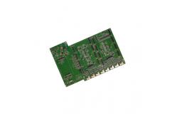
Blind Hole PCB Board Design Carbon Ink Testability Turnkey Pcb Assembly
|
|
Blind - Hole Boards Carbon Ink PCB Board Design Testability Turnkey Assembly
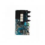
Prototype PCB Assembly Description: 1. Quick-turn prototype PCB assembly.
Prototype PCB Assembly Parameters:
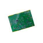
Prototype PCB Assembly Introduction: In high-speed design, the characteristic impedance of controlled impedance boards and lines is one of the most important and common problems. First understand the definition of a transmission line: A transmission line consists of two conductors of a certain length, one for sending a signal and the other for receiving a signal (remember the concept of "loop" instead of "ground"). In a multilayer board, each trace is part of a transmission line, and the adjacent reference plane can act as a second trace or return. The key to a line being a "good" transmission line is to keep its characteristic impedance constant throughout the line. |
||||||||||||||||||||||||||||||||||
| Product Tags: Blind Hole PCB Board Design PCB Board Design Carbon Ink Testability Turnkey Pcb Assembly |
|
Maintainability PCB Board Design Rigid Flex Board Design Gold Finger Plating |

|
Conformal Coating Printed Circuit Board Design Rogers PCB Electronic Board Design |
|
High Tg FR4 PCB Board Design Flexible Multi Layer Board Electronics Device |

|
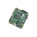
Designability Flex PCB Design 12 SMT Lines 0.3 - 6.5mm Thickness Simple Pcb Design |
|
SMT SMD PCB Design And Assembly Circuit Board Design Online Consumer Electronics |

|
Blind Hole PCB Board Design Carbon Ink Testability Turnkey Pcb Assembly |