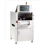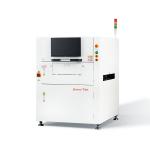
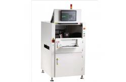
Inline SMT 3D Solder Paste Inspection Machine A510 SMT SPI Machine
|
|
3D SPI can completely solve the problem of shadow and random reflection in the detection process, so that solder paste 3D detection accuracy is higher; equipped with a 5M pixel high-speed camera, detection speed is faster, the image is more delicate and rich; it is an ideal choice for high-speed and high-precision production lines.
TECHNICAL PARAMETERS:
Core Technology and Features
1.PROGRAMMABLE STRUCTURED GRATING PMP IMAGING TECHNOLOGY Phase modulation profiling technology (PMP) is used to achieve three-dimensional measurement of printed solder paste, which can greatly improve measurement accuracy while ensuring high-speed inspection.
2.ACTIVE RGB 2D LIGHT SOURCE,2D LIGHTING SOURCESPatented RGB Tune function takes Red, Green and Blue images and with unique filter algorism, to solve solder bridge detection false alarm and relative zero surface uncertain issue. In the mean time, provide the 2D/3D measurements and image of printed solder paste. ooperate with 2D lighting sources avoids problems caused by the angle of the red RGB color distortion effect in solder; RGB tuning in Different PCB colors is more versatile ; Fulfill a variety of dispensing process testing ; greatly improve the equipment ( height ,volume , area ) epeatability accuracy.
3.HIGH RESOLUTION AND HIGH FRAME RATE IMAGE PROCESSING UNITIt provides a variety of detection accuracy of 2.8μm,4.5μm,5μm,7μm,8μm,10μm,12μm,15μm,18μm,20μm etc. It meets the customer’s requirements for product diversity and detection speed.
4.Z-AXIS DYNAMIC COMPENSATION + TELECENTRIC LENS STATIC COMPENSATIONSolves the problem of ordinary lens, squint and deformation by using high-cost telecentric lens and special software test algorithm, which greatly enhances the inspection accuracy and inspection ability. Achieves the industry's leading static compensation for FPC warping.
5 MINUTES PROGRAMMING AND ONE PRESS OPERATIONEngineers with any levels of experience can independently program the system quickly and accurately through Gerber importing software module and the friendly programming interface. One-button operation by the operator is designed also greatly reduces the requirements for training.
6.APPLICATION OF 3DSPI IN THE FIELD OF HIGH DENSE SOLDER PASTE PRINTING INSPECTIONMiniLED and MicroLED are composed of small LED lights. The number of small LEDs on a single board can reach more than 1 million pads. The size of a single unit of MiniLED is about 100-200μm, while the size of a single unit of MicroLED can be 50μm; therefore, the 3DSPI equipment used in high-dense products uses the highest configuration in the industry; especially the use of marble platforms, linear motors and linear encoder to ensure the movement accuracy of small-sized pads. Using the industry's leading 1.8μm resolution telecentric lens and optimizing Gerber conversion, Load Job, algorithm, data storage and query, etc., the accuracy, speed and efficiency of inspection are greatly improved.
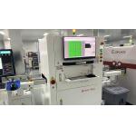
Picture show
|
||||||||||||||||||||||||||||||||||||||||||||||||||||||||||||||||||||
| Product Tags: SMT 3D Solder Paste Inspection Machine Inline 3D Solder Paste Inspection Machine 3D SMT SPI Machine | ||||||||||||||||||||||||||||||||||||||||||||||||||||||||||||||||||||