
1 - 10 of 295
semiconductor device inp wafer
Selling leads

|
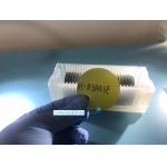
...InP Wafer Indium Phosphide Wafer Semiconductor Substrates 350um 650um Description of InP wafer: InP (Indium phosphide) chips are a commonly used ...
2025-06-18 18:26:53
|

|
...Insulating Indium Phosphide InP Wafer for LD Laser Diode,semiconductor wafer,3inch InP wafer,single crystal wafer2inch 3inch 4inch InP substrates ...
2025-06-18 18:26:48
|

|
Germanium Single Crystals Wafers,Ge optical plates Germanium substrates Application: germanium wafer used in production of semiconductor device, ...
2025-06-18 18:26:50
|

|
4inch 6inch Germanium Single Crystals Ge substrates Wafers,customized Ge optical lens Germanium substrates Application: germanium wafer used in ...
2025-06-18 18:26:49
|

|
4inch 6inch Germanium Single Crystals Ge substrates Wafers,customized Ge optical lens Germanium substrates Application: germanium wafer used in ...
2025-06-18 18:26:51
|

|
...wafer for LeD,semiconducting Gallium Nitride Wafer for ld,GaN template, mocvd GaN Wafer,Free-standing GaN Substrates by Customized size,small size ...
2025-06-18 18:24:19
|
|
... grade SiC substrates,Silicon Carbide substrates for semiconductor device, Application areas 1 high frequency and high power electronic devices ...
2025-06-18 18:22:26
|

|
Product Description Sic Silicon Carbide Semiconductor Devices Multiple Crystal Forms 4H 6H 3C Custom Size 5G Communication Chips A silicon carbide ...
2025-06-18 18:23:53
|

|
...InP indium Phosphide Wafer 4inch Semi-Insulating Indium Phosphide InP Wafer for LD Laser Diode,semiconductor wafer,3inch InP wafer,single crystal ...
2025-06-18 18:26:50
|

|
..., semiconductor wafer, InP Laser Epitaxial Wafer Features of InP Laser Epitaxial Wafer - use InP wafers to manufacture - support customized ones ...
2025-06-18 18:26:55
|