
51 - 60 of 309
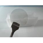
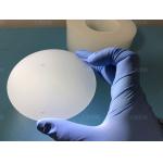
ssp sapphire substrate wafer
Selling leads
|
...supplier of sapphire substrates for photoelectronic applications, including the high brightness LED market. The material is grown and orientated, ...
2025-08-01 00:08:35
|
|
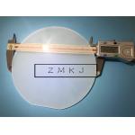
... dia150mm C-plane Sapphire SSP/DSP wafers with 650um/1000um Thicknessdiameter300mm 12inch Al2O3 Sapphire wafers carrier with notch SSP DSP 1.0mm C ...
2025-05-06 20:40:26
|
|
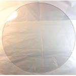
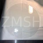
...Sapphire Wafers Thickness 0.175mm/0.3mm/0.4mm/0.5mm Dsp 2 Inch C Plane Polished Sapphire Wafers Crystal Substrates The specifications of 2inch ...
2025-08-01 00:08:35
|
|
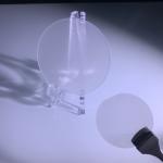
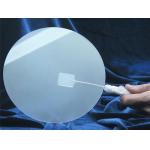
Ultra-thin 2inch sapphire DSP wafers thickness 100um 0.1mm 2inch 100um Ultra Thin sapphire wafers 0.1mm Thickness C-plane DSP Sapphire wafer Why ...
2025-05-06 20:38:59
|
|
... Carrier wafers for SOS GaAs epitaxy About synthetic sapphire crystal The Kyropoulos process (KY process) for sapphire crystal growth is currently ...
2025-05-06 20:38:48
|
|
...KY process) for sapphire crystal growth is currently used by many companies in China to produce sapphire for the electronics and optics industries. ...
2025-05-06 20:38:39
|
|
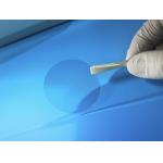
Sapphire wafer 8inch Diameter 200mm C Plane A Plane KY EFG Double Slide Polished Product Description: In 1992, Japanese engineer Shuji Nakamura ...
2025-05-06 20:39:56
|
|
8inch/6inch/5inch/ 2inch /3inch 4inch /5inch C-axis/ a-axis/ r-axis/ m-axis 6"/6inch dia150mm C-plane Sapphire SSP/DSP wafers with 650um/1000um ...
2025-05-06 20:38:46
|
|
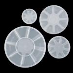
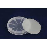
...Wafer Carrier, Single Wafer Sample Box for Silicon, Sapphire, SiC Substrate Cleanroom Class 100 Grade 1 inch Style Single Wafer Carrier Shipper box ...
2025-05-06 20:47:34
|
|
...substrates template,GaN wafer for LeD,semiconducting Gallium Nitride Wafer for ld,GaN template, mocvd GaN Wafer,Free-standing GaN Substrates by ...
2025-05-06 20:44:30
|