
31 - 40 of 369
single crystal semiconductor substrate
Selling leads
|
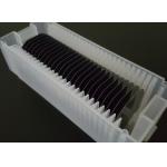
... The Kyropoulos process (KY process) for sapphire crystal growth is currently used by many companies in China to produce sapphire for the ...
2025-05-06 20:39:27
|
|
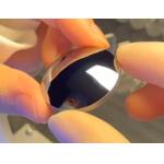
...crystals crystal substrate TeO2 wafer TeO2 Crystal & Q Switch TeO2 is an excellent ascousto-optic (AO) crystal with high AO figure of merit, ...
2025-05-06 20:40:28
|
|
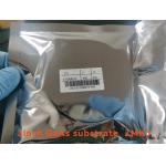
...Substrate/Wafers (150mm, 200mm) Silicon Carbide Ceramic Excellent CorrosionSingle crystal single side polished silicon wafer sic wafer polishing ...
2025-05-06 20:41:07
|
|
...substrate Properties of GaN Chemical properties of GaN 1) At room temperature, GaN is insoluble in water, acid and alkali. 2)Dissolved in a hot ...
2025-05-06 20:44:40
|
|
... (GaAs) Gallium Arsenide Wafers Gallium arsenide (GaAs) is a compound of the elements gallium and arsenic. It is a III-V direct bandgap semiconduct...
2025-05-06 20:44:31
|
|
... (GaAs) Gallium Arsenide Wafers Gallium arsenide (GaAs) is a compound of the elements gallium and arsenic. It is a III-V direct bandgap semiconduct...
2025-05-06 20:44:43
|
|
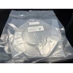
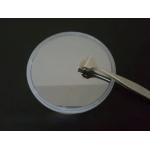
8inch Dia200mm C-Plane Al2O3 99.999% Sapphire Single Crystal Wafer Carrier Substrate 1sp 2sp *, *::before, *::after {box-sizing: border-box; } * ...
2025-07-28 00:08:52
|
|
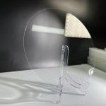
12Inch 300mm Thickness 1.0mm Sapphire Wafers Substrate Ssp Dsp C-Plane Single Crystal 99.999% Al2O3 Sapphire wafers are known for their exceptional ...
2025-07-28 00:08:52
|
|
...-N 4inch 6inch dia 150mm silicon carbide single crystal (sic) substrates wafersS/ Customzied as-cut sic wafers About Silicon Crystal * Low ...
2025-07-28 00:08:51
|
|
...Semiconductor Substrate For Epitaxial Growth VGF 2inch 4inch 6inch n-type prime grade GaAs wafer for epitaxial growth Gallium arsenide can be made ...
2025-05-06 20:45:00
|