
181 - 190 of 251
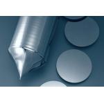
optical silicon carbon wafers
Selling leads
|
...wafers for GaN epitaxial growth;0.1mm/100um 2inch sapphire c-axis substrates TYPICAL CHOICES FOR PART ORIENTATION: Why Sapphire? Zero Degree: The ...
2025-05-06 20:38:43
|
|
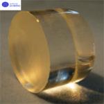
...Tellurium oxide (TeO2) crystals crystal substrate TeO2 wafer TeO2 Crystal & Q Switch TeO2 is an excellent ascousto-optic (AO) crystal with high AO ...
2025-05-06 20:40:28
|
|
...:Lithium tantalate (LiTaO3) single crystal has a very good electro-optical, piezoelectric and pyroelectric properties, widely used in pyroelectric ...
2025-05-06 20:44:34
|
|
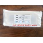
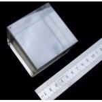
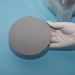
C-axis (0001) orientation 12inch diameter 300mm with notch DSP Sapphire Substrate wafers thickness 1.5mm C-a Diameter 8inch 12inch dia300mm polished ...
2025-05-06 20:38:54
|
|
...wafers Germanium substrate Ge window for infrared Co2 lasers Ge Material Introduce Among optical materials, germanium materials are increasingly ...
2025-05-06 20:44:48
|
|
...wafers Germanium substrate Ge window for infrared Co2 lasers Ge Material Introduce Among optical materials, germanium materials are increasingly ...
2025-05-06 20:44:49
|
|
...wafer High-Frequency SAW Filters High Piezoelectric Coefficient Introduce Lithium Tantalate (LiTaO₃) is a ferroelectric crystal that has attracted ...
2025-05-29 00:09:29
|
|
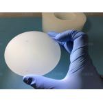
... Carrier wafers for SOS GaAs epitaxy About synthetic sapphire crystal The Kyropoulos process (KY process) for sapphire crystal growth is currently ...
2025-05-06 20:38:48
|
|
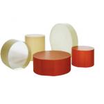
...axis 6"/6inch dia150mm C-plane Sapphire SSP/DSP wafers with 650um/1000um Thicknessdiameter300mm 12inch Al2O3 Sapphire wafers carrier with notch SSP ...
2025-05-06 20:40:26
|
|
... 4inch 6inch sapphire substrates wafers for GaN epitaxial growth;0.1mm/100um 2inch sapphire c-axis substrates TYPICAL CHOICES FOR PART ORIENTATION: ...
2025-05-06 20:38:52
|