
21 - 30 of 46
laser device gallium nitride wafer
Selling leads
|
dia50.8mm 2inch 1inch AlN substrate/AlN single crystal wafers 10x10mm or diameter 10mm dia25.4mm dia30mm, dia45mm, dia50.8mm AlN substrate AlN single ...
2025-05-06 20:44:42
|
|
...Nitride Template on 430um sapphire/ 350um Sic substrates AlN Wafer Characteristic III-Nitride(GaN,AlN,InN) 2inch AlN template on sapphire or sic ...
2025-05-06 20:44:29
|
|
... Wafer Characteristic III-Nitride(GaN,AlN,InN) Gallium Nitride is one kind of wide-gap compound semiconductors. Gallium Nitride (GaN) substrate is ...
2025-05-06 20:44:18
|
|
Product Description: Our InP (Indium Phosphide) wafers are renowned for their low defect density and high performance, widely used in optoelectronics ...
2025-05-06 20:44:24
|
|
8inch GaN-on-Si Epitaxy Wafer 110 111 110 N-type P-type Customization Semiconductor RF LED Description of GaN-on-Si Wafers: The 8-inch-diameter GaN-on...
2025-05-06 20:44:26
|
|
Product Description: Our InP (Indium Phosphide) semiconductor wafers, renowned for their exceptional electronic and optoelectronic properties, have ...
2025-05-06 20:44:23
|
|
AlN on Diamond template wafers AlN epitaxial films on Diamond substrate AlN on Sapphire /AlN-on-SiC/ AlN-ON Silicon Welcome to Know AlN Template on ...
2025-05-06 20:44:22
|
|
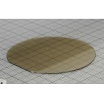
...Sapphire Substrate wafers thickness 1.15mm C-a Sapphire application Application Sapphire wafer and substrate applications include: Microelectronic ...
2025-05-06 20:40:27
|
|
10x10mmt Terbium gallium garnet (TGG)crystals substrate wafer for laser device Product Type: Yttrium aluminum garnet (YAG) is an isotropic crystal ...
2025-08-03 00:08:11
|
|
...wafer 4H N-Type CVD Orientation : 4.0°±0.5° Semi-Insulating 3-Inch Silicon Carbide wafer's Abstract The unique electronic and thermal properties of ...
2025-05-06 20:41:19
|