
21 - 30 of 50
hvpe gallium nitride wafer
Selling leads
|
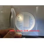
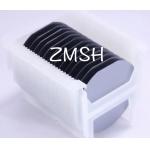
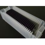
...wafer for LeD, semiconducting Gallium Nitride Wafer for ld, GaN template, mocvd GaN Wafer,Free-standing GaN Substrates by Customized size, small ...
2025-05-06 20:44:15
|
|
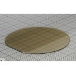
dia50.8mm 2inch 1inch AlN substrate/AlN single crystal wafers 10x10mm or diameter 10mm dia25.4mm dia30mm, dia45mm, dia50.8mm AlN substrate AlN single ...
2025-05-06 20:44:42
|
|
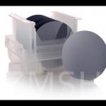
8inch GaN-on-Si Epitaxy Wafer 110 111 110 N-type P-type Customization Semiconductor RF LED Description of GaN-on-Si Wafers: The 8-inch-diameter GaN-on...
2025-05-06 20:44:26
|
|
Product Description: Our InP (Indium Phosphide) semiconductor wafers, renowned for their exceptional electronic and optoelectronic properties, have ...
2025-05-06 20:44:23
|
|
Product Description: Our InP (Indium Phosphide) wafers are renowned for their low defect density and high performance, widely used in optoelectronics ...
2025-05-06 20:44:24
|
|
AlN on Diamond template wafers AlN epitaxial films on Diamond substrate AlN on Sapphire /AlN-on-SiC/ AlN-ON Silicon Welcome to Know AlN Template on ...
2025-05-06 20:44:22
|
|
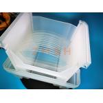
...Sapphire Substrate wafers thickness 1.15mm C-a Sapphire application Application Sapphire wafer and substrate applications include: Microelectronic ...
2025-05-06 20:40:27
|
|
...Gallium arsenide GaAs Wafer Product Description (GaAs) Gallium Arsenide Wafers PWAM Develops and manufactures compound semiconductor substrates...
2025-05-06 20:44:31
|
|
... (GaAs) Gallium Arsenide Wafers Gallium arsenide (GaAs) is a compound of the elements gallium and arsenic. It is a III-V direct bandgap semiconduct...
2025-05-06 20:44:31
|
|
... (GaAs) Gallium Arsenide Wafers Gallium arsenide (GaAs) is a compound of the elements gallium and arsenic. It is a III-V direct bandgap semiconduct...
2025-05-06 20:44:43
|