
231 - 240 of 315
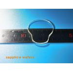
dsp sapphire substrate wafers
Selling leads
|
10x10mmt/Tellurium oxide (TeO2) crystals crystal substrate TeO2 wafer TeO2 Crystal & Q Switch TeO2 is an excellent ascousto-optic (AO) crystal with ...
2025-05-06 20:40:28
|
|
4inch N-type Ge wafers Germanium substrate Ge window for infrared Co2 lasers Ge Material Introduce Among optical materials, germanium materials are ...
2025-05-06 20:44:48
|
|
4inch N-type Ge wafers Germanium substrate Ge window for infrared Co2 lasers Ge Material Introduce Among optical materials, germanium materials are ...
2025-05-06 20:44:49
|
|
... as the foundation for high-performance semiconductor devices. Crafted with advanced float-zone mono-crystalline silicon technology, this substrate ...
2025-05-06 20:45:11
|
|
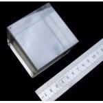
transparent customized size sapphire optical window Customize sapphire optical window pieces according to requirements monocrystalline Synthetic ...
2025-05-06 20:37:46
|
|
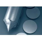
...wafer 1mm thickness for ingot growth Customzied size/2inch/3inch/4inch/6inch 6H-N/4H-SEMI/ 4H-N SIC ingots/High purity 4H-N 4inch 6inch dia 150mm ...
2025-05-06 20:42:04
|
|
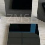
Quartz Wafer Quartz Wafers 2", 3", 4", 6", 8", 12" SiO₂ Semiconductor Optical Introduction of Quartz Wafer Quartz wafers ...
2025-07-10 18:23:14
|
|
...-sized substrates that play a crucial role in various semiconductor applications. Commonly used in compact electronic devices where space is ...
2025-05-06 20:41:38
|

|
Si wafer 4inch Polished CZ Dopant Arsenic(As) Boron(B) Phosphorus(Ph) (100) Semiconductor Describe of Si Wafer: A Silicon wafer is a very thin round ...
2025-05-06 20:45:29
|
|
2inch 4inch 6inch 8inch 12inch Si wafer Silicon wafer Polishing Undoped P type N type Semiconductor Description of Si Wafer: Silicon wafer is a ...
2025-05-06 20:45:33
|