
41 - 50 of 59
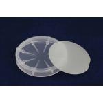
customized lsao substrate
Selling leads
|
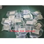
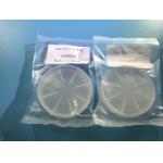
...substrates template,GaN wafer for LeD,semiconducting Gallium Nitride Wafer for ld,GaN template, mocvd GaN Wafer,Free-standing GaN Substrates by ...
2025-05-06 20:44:30
|
|
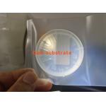
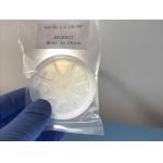
...substrates template,GaN wafer for LeD,semiconducting Gallium Nitride Wafer for ld,GaN template, mocvd GaN Wafer,Free-standing GaN Substrates by ...
2025-05-06 20:44:21
|
|
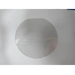
...substrates template,GaN wafer for LeD,semiconducting Gallium Nitride Wafer for ld,GaN template, mocvd GaN Wafer,Free-standing GaN Substrates by ...
2025-05-06 20:44:12
|
|
...substrates template,GaN wafer for LeD,semiconducting Gallium Nitride Wafer for ld,GaN template, mocvd GaN Wafer,Free-standing GaN Substrates by ...
2025-05-06 20:44:13
|
|
...substrates template,GaN wafer for LeD,semiconducting Gallium Nitride Wafer for ld,GaN template, mocvd GaN Wafer,Free-standing GaN Substrates by ...
2025-05-06 20:44:28
|
|
...substrates template,GaN wafer for LeD,semiconducting Gallium Nitride Wafer for ld,GaN template, mocvd GaN Wafer,Free-standing GaN Substrates by ...
2025-05-06 20:44:15
|
|
...substrates template,GaN wafer for LeD, semiconducting Gallium Nitride Wafer for ld, GaN template, mocvd GaN Wafer,Free-standing GaN Substrates by ...
2025-05-06 20:44:15
|

|
...substrates template,GaN wafer for LeD,semiconducting Gallium Nitride Wafer for ld,GaN template, mocvd GaN Wafer,Free-standing GaN Substrates by ...
2025-05-06 20:44:20
|
|
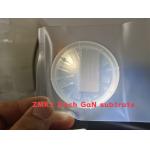
... on the market for 2 inch and 3 inch Research grade SiC substrate wafers. SiC substrate wafers have a variety of applications in electronic device ...
2025-07-17 00:10:50
|
|
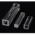
High purityJGS2 JGS1 quartz tube with various customized thickness size and shape High Temperature Quartz Tube We are a manufacturer of Transparent ...
2025-05-06 20:38:53
|