
8-Inch SiC Epitaxial Wafers Yield And Efficiency Scalable Power Electronics
|
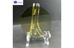
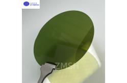
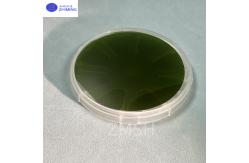
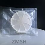
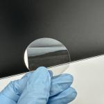
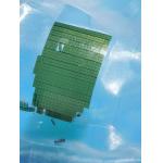
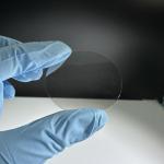
SiC Epitaxial Wafer Overview8-inch (200 mm) SiC Epitaxial Wafers are now emerging as the most advanced form factor in the SiC industry. Representing the cutting edge of material science and manufacturing capability, 8” SiC epitaxial wafers offer unparalleled opportunities for scaling up power device production while driving down the cost per device. As demand for electric vehicles, renewable energy, and industrial power electronics continues to surge globally, 8” wafers are enabling a new generation of SiC MOSFETs, diodes, and integrated power modules with higher throughput, better yield, and lower manufacturing costs. With wide bandgap properties, high thermal conductivity, and exceptional breakdown voltage, 8” SiC wafers are unlocking new levels of performance and efficiency in advanced power electronics.
How 8” SiC Epitaxial Wafers Are Made
Manufacturing 8” SiC epitaxial wafers requires next-generation CVD reactors, precise crystal growth control, and ultra-flat substrate technology:
Specifications
Applications8” SiC epitaxial wafers enable mass production of reliable power devices in sectors including:
Frequently Asked Questions (FAQ)1. What is the benefit of 8” SiC wafers? 2. How mature is 8” SiC production? 3. Can doping and thickness be customized? 4. Are existing fabs compatible with 8” SiC wafers? 5. What is typical lead time? 6. What industries will adopt 8” SiC fastest?
Related Products
12 inch SiC Wafer 300mm Silicon Carbide wafer Conductive Dummy Grade N-Type Research grade
4H/6H P-Type Sic Wafer 4inch 6inch Z Grade P Grade D Grade Off Axis 2.0°-4.0° Toward P-type Doping |
||||||||||||||||||||||||||||||||||||||||||||||||||||||||||||||||||||||||||||||||||||||||||||||||||||||||||||||||||||||||||||||||||||||||||||||||||||
| Product Tags: Epitaxial SiC Wafers 8 Inch SiC Epitaxial Wafer |
|
High Purity Semi-Insulating HPSI SiC Powder/99.9999% Purity Crystal Growth |
|
Semi-Insulating SiC Wafers 3inch 76.2mm 4H Type SiC For Semiconductors |
|
High Resistivity 8inch 200mm Silicon Carbide Wafer Production Grade 4H-N |
|
4H/6H Semi-Insulating Silicon Carbide Wafer For Production/Research/Dummy Grade |
|
Square SiC Windows Silicon Carbide Substrate 1x1x0.5mmt SiC Lens |
|
Semi Insulating Silicon Carbide Wafer SiC Substrate Orientation 0001 Bow/Warp ≤50um |