
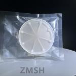
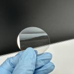
Solid SiC Vacuum Chuck – Ultra-Flat Carrier Plate for Thin Wafer Processing
|
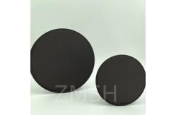
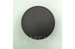
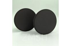
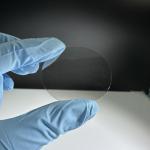
Introduction Of SiC Vacuum ChuckThe ultra-flat ceramic wafer vacuum chuck is made with high-purity silicon carbide (SiC) coating, designed for advanced wafer handling processes. Optimized for use in MOCVD and compound semiconductor growth equipment, it offers excellent heat and corrosion resistance, ensuring exceptional stability in extreme processing environments. This contributes to improved yield management and reliability in semiconductor wafer fabrication. Its low-surface-contact configuration helps minimize backside particle contamination, making it ideal for highly sensitive wafer applications where cleanliness and precision are critical. This solution combines high performance with cost-efficiency, supporting demanding manufacturing environments with reliable and long-lasting performance.
Working Principle Of SiC Vacuum Chuck
In high-temperature processes, the SiC carrier plate serves as a support to carry wafers or thin-film materials. Its high thermal conductivity ensures uniform heat distribution, improving process stability and uniformity. Additionally, due to its hardness and chemical inertness, the plate maintains structural integrity even in corrosive environments, ensuring product purity and equipment safety.
Parameters of Wafer Vacuum Chuck
Features of Wafer Vacuum Chuck ● Ultra-flat capabilities ● Mirror polish ● Exceptional light weight ● High stiffness ● Low thermal expansion ● Φ 300 mm diameter and beyond ● Extreme wear resistance
Applications of SiC Porous Vacuum ChuckIn the semiconductor and optoelectronic industries, ultra-thin wafers are often placed on porous silicon carbide (SiC) vacuum chucks. By connecting to a vacuum generator, negative pressure is applied to securely hold the wafer in place without mechanical clamps. This enables precise and stable processing during the following stages:
The use of a high-purity, porous SiC vacuum chuck ensures excellent thermal and chemical stability throughout these processes, while minimizing contamination and maintaining wafer flatness. Its superior mechanical strength and thermal conductivity also reduce the risk of wafer breakage during processing, especially for fragile or ultra-thin substrates like GaAs, InP, or SiC.
Frequently Asked Questions (FAQ) – SiC Porous Vacuum Chuck
Q1: What is the main purpose of a porous SiC vacuum chuck?
Q2: What materials can be processed using a SiC vacuum chuck?
Q3: What is the advantage of using porous SiC over metal or ceramic
chucks?
Related Products
12 inch SiC Wafer 300mm Silicon Carbide wafer Conductive Dummy Grade N-Type Research grade
4H/6H P-Type Sic Wafer 4inch 6inch Z Grade P Grade D Grade Off Axis 2.0°-4.0° Toward P-type Doping |
|||||||||||||||||||||||||||||||||||||||
| Product Tags: Corrosion Resistance SiC Carrier Plate Thermal Conductivity SiC Carrier Plate MOCVD SiC Carrier Plate | |||||||||||||||||||||||||||||||||||||||
|
High Purity Semi-Insulating HPSI SiC Powder/99.9999% Purity Crystal Growth |
|
Semi-Insulating SiC Wafers 3inch 76.2mm 4H Type SiC For Semiconductors |
|
High Resistivity 8inch 200mm Silicon Carbide Wafer Production Grade 4H-N |
|
4H/6H Semi-Insulating Silicon Carbide Wafer For Production/Research/Dummy Grade |
|
Square SiC Windows Silicon Carbide Substrate 1x1x0.5mmt SiC Lens |
|
Semi Insulating Silicon Carbide Wafer SiC Substrate Orientation 0001 Bow/Warp ≤50um |