
31 - 40 of 58
semiconductor molybdenum sputtering target
Selling leads
|
... implantation (doping), which aims to obtain specific electrical conductivity properties. Ion sources used to emit ion beams are made of tungsten ...
2024-12-09 20:38:34
|
|
|
... implantation (doping), which aims to obtain specific electrical conductivity properties. Ion sources used to emit ion beams are made of tungsten ...
2024-12-09 22:00:03
|

|
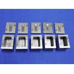
Ion Implantation Molybdenum Parts For Semiconductor Products Application: Semiconductor ion implantation is a new technology of material surface ...
2024-12-09 20:38:34
|
|
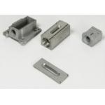
High Pure ASTM B387 Molybdenum Semiconductor Ion Implanation Parts Application: Semiconductor ion implantation is a new technology of material surface ...
2024-12-09 20:39:36
|
|
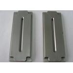
... used in the doping of semiconductor materials, the surface modification of metals, ceramics, polymers etc. It is a necessary technique in the ...
2024-12-09 20:50:01
|
|
|
High Pure ASTM B387 Molybdenum Semiconductor Ion Implanation Parts Application: Semiconductor ion implantation is a new technology of material surface ...
2024-12-09 22:00:03
|
|
|
... used in the doping of semiconductor materials, the surface modification of metals, ceramics, polymers etc. It is a necessary technique in the ...
2026-05-20 00:15:40
|
|
|
Ion Implantation Molybdenum Parts For Semiconductor Products Application: Semiconductor ion implantation is a new technology of material surface ...
2024-12-09 22:00:03
|
|
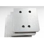
... Molybdenum plate can be used as electro-optic source, high temperature structural parts, high temperature heat insulation screen, target, etc. ...
2024-12-09 20:41:40
|
|
|
... Molybdenum plate can be used as electro-optic source, high temperature structural parts, high temperature heat insulation screen, target, etc. ...
2026-05-20 00:15:40
|