
11 - 20 of 30
semiconductor moly sputtering target
Selling leads

|
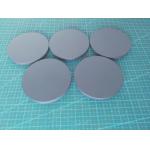
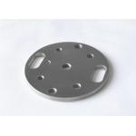
...Target used for thin film solar cells new energy Sputtering is a new type of Physical Vapor Deposition (PVD) method. Sputtering is widely used in: ...
2025-07-01 00:11:52
|
|
High Purity 99.99% ITO Targets In2O3:SnO2=90:10 wt% Application In terms of application, ITO transparent conductive film glass is mainly used in LCD ...
2024-12-09 20:26:58
|
|
|
High Purity 99.99% ITO Targets In2O3:SnO2=90:10 wt% Application In terms of application, ITO transparent conductive film glass is mainly used in LCD ...
2024-12-09 22:00:03
|
|
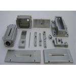
...Semiconductor Ion Implantation Accessories Tungsten Ion implantation parts are a new generation of high technology for material surface treatment. ...
2024-12-09 20:41:40
|
|
|
...Semiconductor Ion Implantation Accessories Tungsten Ion implantation parts are a new generation of high technology for material surface treatment. ...
2025-07-01 00:11:52
|
|
... 5. Application Capacitors, high-temperature furnace parts, semiconductor, sputtering targets 6. Strict quality control System: Each link of the ...
2024-12-09 19:37:28
|
|
...ts, semiconductor, sputtering targets 6. Strict quality control System: Each link of the production will be strickly controled,ensuring without one ...
2024-12-09 19:37:28
|
|
|
...ts, semiconductor, sputtering targets 6. Strict quality control System: Each link of the production will be strickly controled,ensuring without one ...
2024-12-09 22:00:03
|
|
|
... 5. Application Capacitors, high-temperature furnace parts, semiconductor, sputtering targets 6. Strict quality control System: Each link of the ...
2024-12-09 22:00:03
|
|
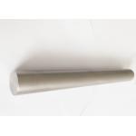
Molybdenum Crucible As per Drawing Specification: Product Name 99.95% Min Purity High Temperature Resistant Molybdenum Machined Parts Standard ASTM ...
2024-12-09 19:37:44
|