
261 - 270 of 331
technical ceramic sputtering target
Selling leads
|
Terbium scandium aluminum garnet (TSAG) crystal Terbium scandium aluminum garnet (TSAG) crystal is an ideal magneto-optical material, suitable for ...
2024-12-09 13:42:48
|
|
Laser crystal YAG YAG is an earlier laser crystal. Because of its good basic properties, Nd: YAG is still widely used in near and far infrared solid...
2024-12-09 13:42:48
|
|
CE doped gadolinium aluminum gallium garnet (CE: GAGG), Scintillation crystal Cerium doped gadolinium aluminum gallium garnet (CE: GAGG) is a kind of ...
2024-12-09 13:42:48
|
|
CE: luage, Scintillation crystal CE: luage: luag is an excellent scintillator with fast attenuation (80ns), high light yield and 510nm emission peak, ...
2024-12-09 13:42:48
|
|
Piezoelectric crystal, LGS LGS is a kind of multifunctional crystal with excellent properties. The dielectric, elastic and piezoelectric constants of ...
2024-12-09 13:42:48
|
|
Gadolinium gallium garnet (GGG) substrate, an excellent substrate material for Bi Fe garnet epitaxial films Gadolinium gallium garnet (GGG) substrate, ...
2024-12-09 13:42:48
|
|
LaAlO3 single crystal LaAlO3 single crystal is the most important industrial and large-scale high temperature superconducting thin film substrate ...
2024-12-09 13:42:48
|
|
Gadolinium gallium garnet (GGG) In optical communication equipment, 1.3 μ And 1.5 μ The core part of the optical isolator is YIG or big film placed in ...
2024-12-09 13:42:48
|
|
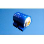
Faraday Rotator Faraday rotator is based on the nonreciprocity of magneto-optical materials, that is, it can rotate the polarization planes of the ...
2024-12-09 13:42:48
|
|
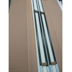
Disilicide-molybdenum heaters Disilicide-molybdenum heaters used in sintering of ferrites, technical ceramics and refractories; glass industry ...
2024-12-09 19:40:24
|