
21 - 30 of 50
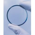
single crystal gallium phosphide
Selling leads
|
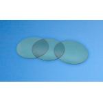
...Gallium Antimonide ) We provides GaSb wafer ( Gallium Antimonide ) to optoelectronics industry in diameter up to 2 inch . GaSb crystal is a ...
2024-12-09 19:40:24
|
|
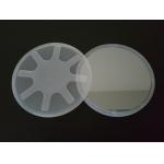
...gallium garnet (GGG) substrate, an excellent substrate material for Bi Fe garnet epitaxial films Gadolinium gallium garnet (GGG) substrate, one of ...
2024-12-09 13:42:48
|
|
|
...gallium garnet (GGG) substrate, an excellent substrate material for Bi Fe garnet epitaxial films Gadolinium gallium garnet (GGG) substrate, one of ...
2024-12-09 19:40:24
|
|
LaAlO3 single crystal LaAlO3 single crystal is the most important industrial and large-scale high temperature superconducting thin film substrate ...
2024-12-09 13:42:48
|
|
|
LaAlO3 single crystal LaAlO3 single crystal is the most important industrial and large-scale high temperature superconducting thin film substrate ...
2024-12-09 19:40:24
|
|
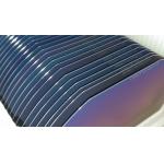
...crystals Semiconductor group diamond single crystal products have the advantages of large bandgap, low electron saturation velocity, large carrier ...
2025-06-29 00:31:29
|
|
... conductivity make it an ideal material for Raman laser crystals. Our company provides single crystal diamond Raman crystals of various specificati...
2025-06-29 00:31:29
|
|
... and opto-electronics industry in diameter range from 2 inch to 4 inch We are a worldwide supplier of single crystal Ge wafer ( Germanium wafer ) ...
2024-12-09 13:28:02
|
|
|
... and opto-electronics industry in diameter range from 2 inch to 4 inch We are a worldwide supplier of single crystal Ge wafer ( Germanium wafer ) ...
2024-12-09 19:40:24
|
|
... is 30 mm . II-VI compound wafer are compounds formed by elements from II &VI group of the periodic table,Normally the crystal is as-grown crystal ...
2024-12-09 13:28:02
|